CAN
Features and benefits
         2.1 General

        • Fully ISO 11898-2:2016, SAE J2284-1 to SAE J2284-5 and SAE J1939-14 compliant

        • Timing guaranteed for data rates up to 5 Mbit/s in the CAN FD fast phase

        • Suitable for 12 V and 24 V systems

        • Low Electromagnetic Emission (EME) and high Electromagnetic Immunity (EMI),

        according to proposed EMC Standards IEC 62228-3 and SAE J2962-2

        • Variants with a V pin allow for direct interfacing with 3.3 V to 5 V microcontrollers

        • Shorter propagation delay on the TJA1042B and TJA1042C variants supports larger

        network topologies (see Table 8)

        • SPLIT voltage output on TJA1042T and TJA1042CT for stabilizing the recessive bus

        level

        • Both V and non-V variants are available in SO8 and leadless HVSON8 (3.0 mm

        IO IO

        × 3.0 mm) packages; HVSON8 with improved Automated Optical Inspection (AOI)

        capability.

        • Dark green product (halogen free and Restriction of Hazardous Substances (RoHS)

        compliant)

        • AEC-Q100 qualified

        2.2 Predictable and fail-safe behavior

        • Very low-current Standby mode with host and bus wake-up capability

        • Functional behavior predictable under all supply conditions

        • Transceiver disengages from the bus (high-ohmic) when the supply voltage drops

        below the switch-off undervoltage threshold

        • Transmit Data (TXD) dominant time-out function

        • Bus-dominant time-out function in Standby mode

        • Undervoltage detection on pins V and V

        CC IO

        2.3 Protections

        • High ESD handling capability on the bus pins (±8 kV)

        • High voltage robustness on CAN pins (±58 V)

        • Bus pins protected against transients in automotive environments

        • Thermally protected
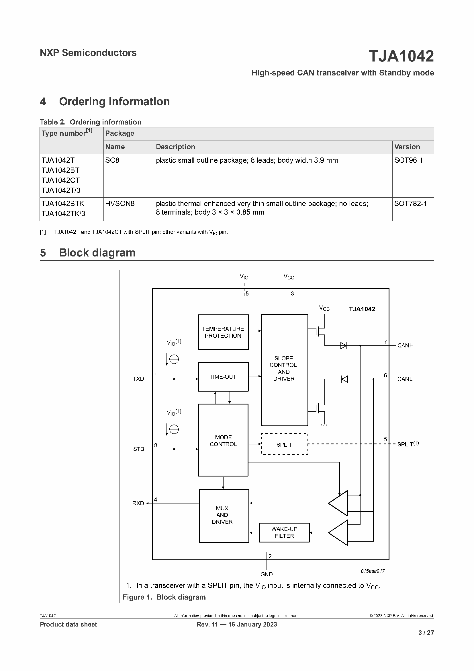
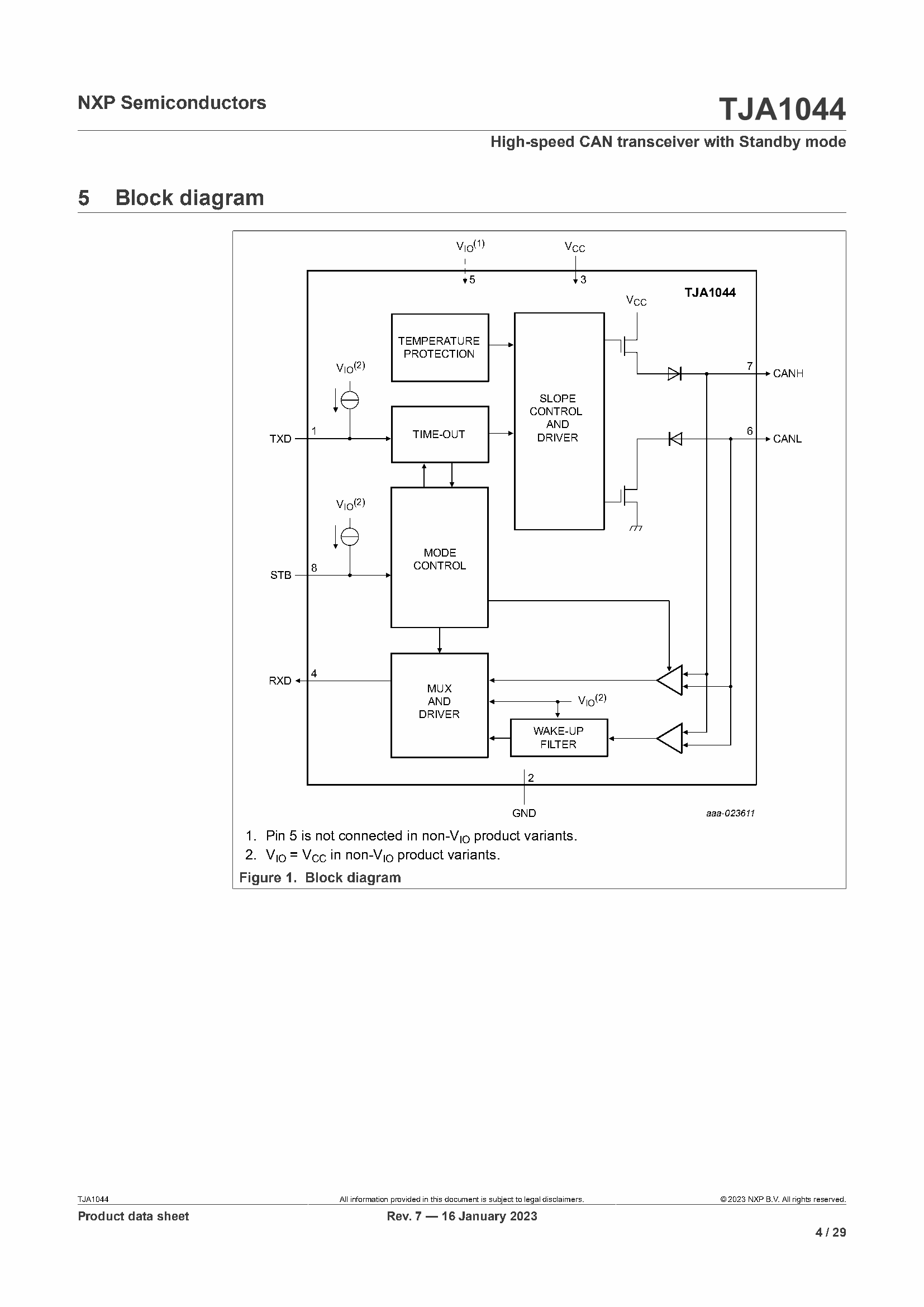
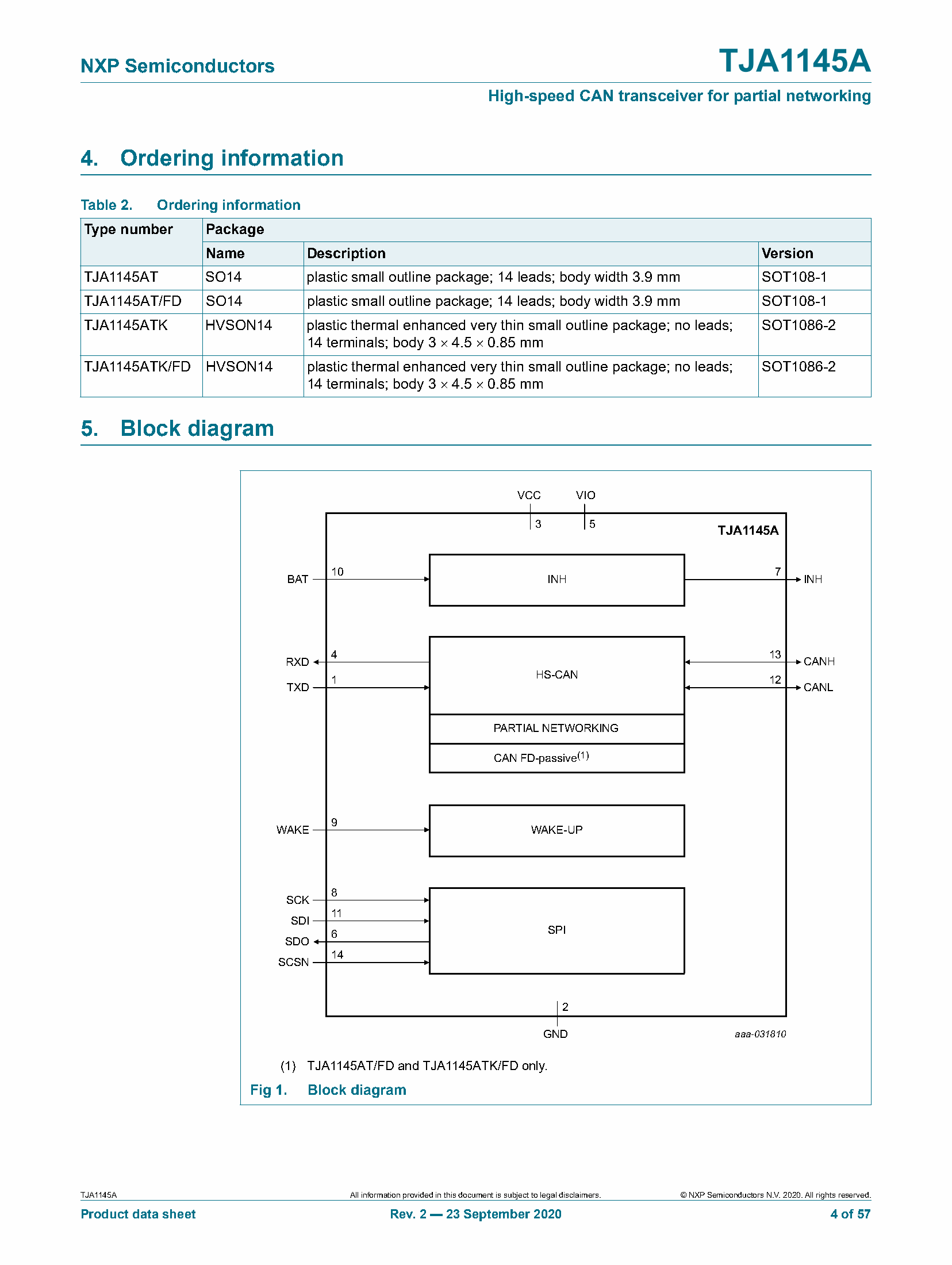
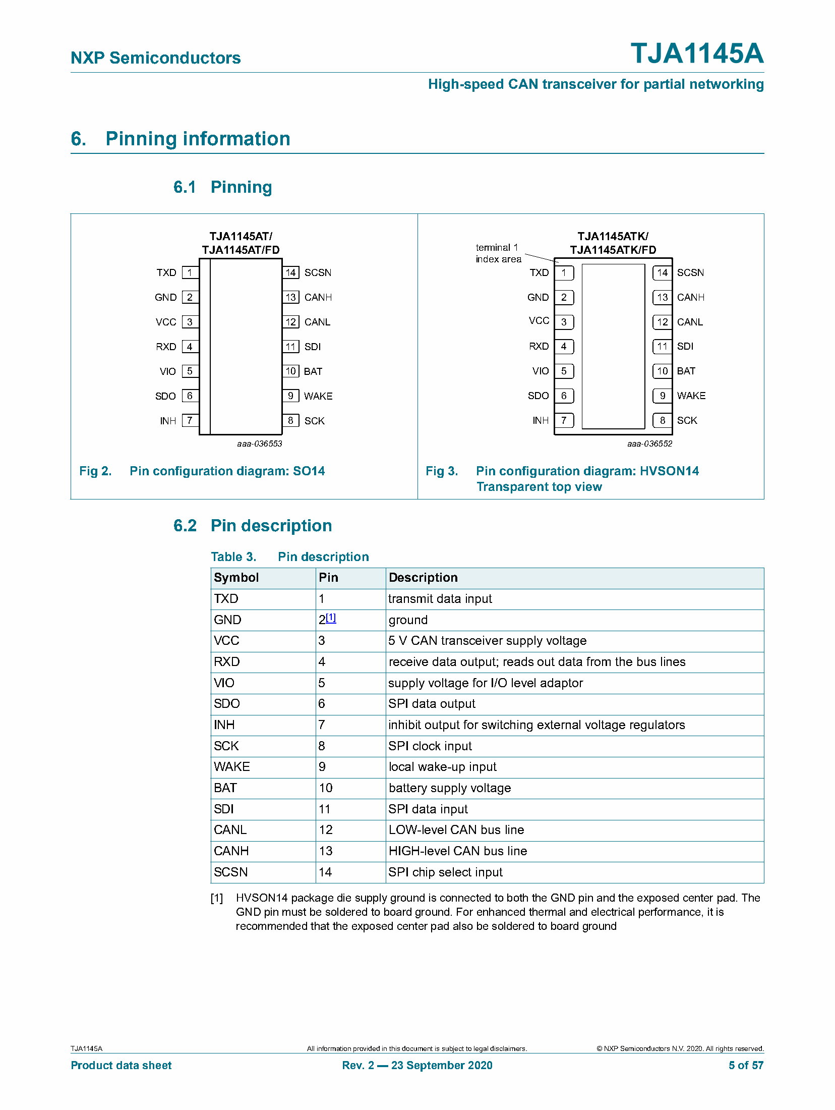
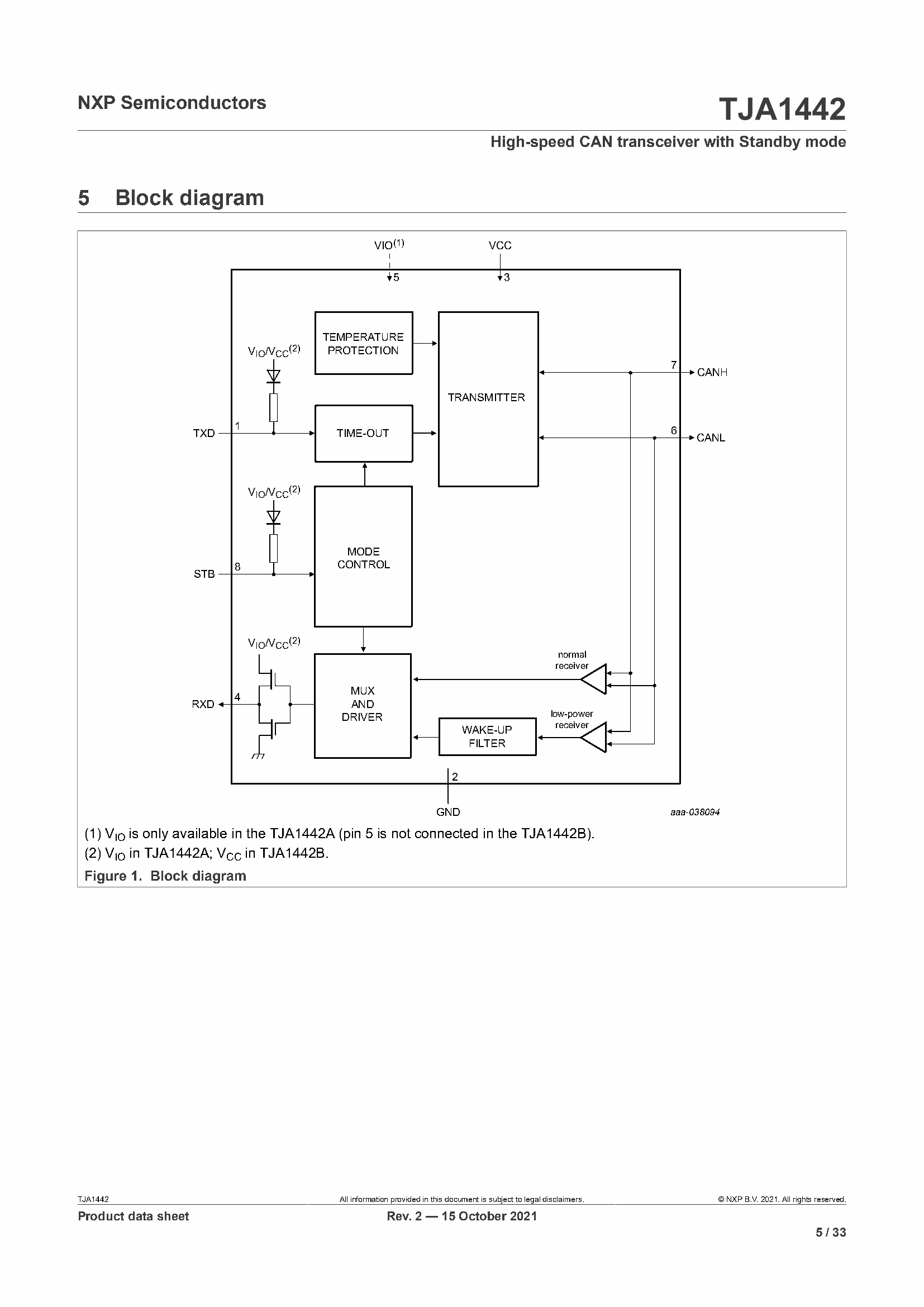
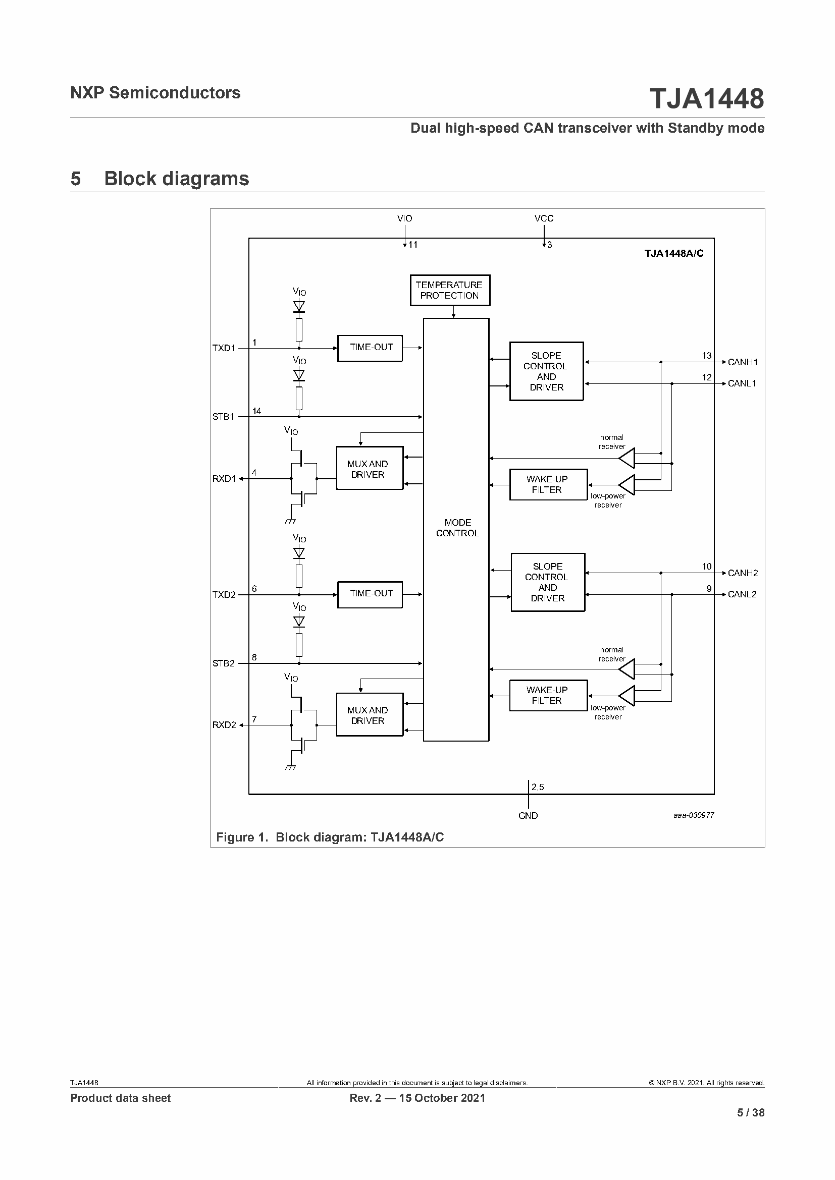
Block Digram
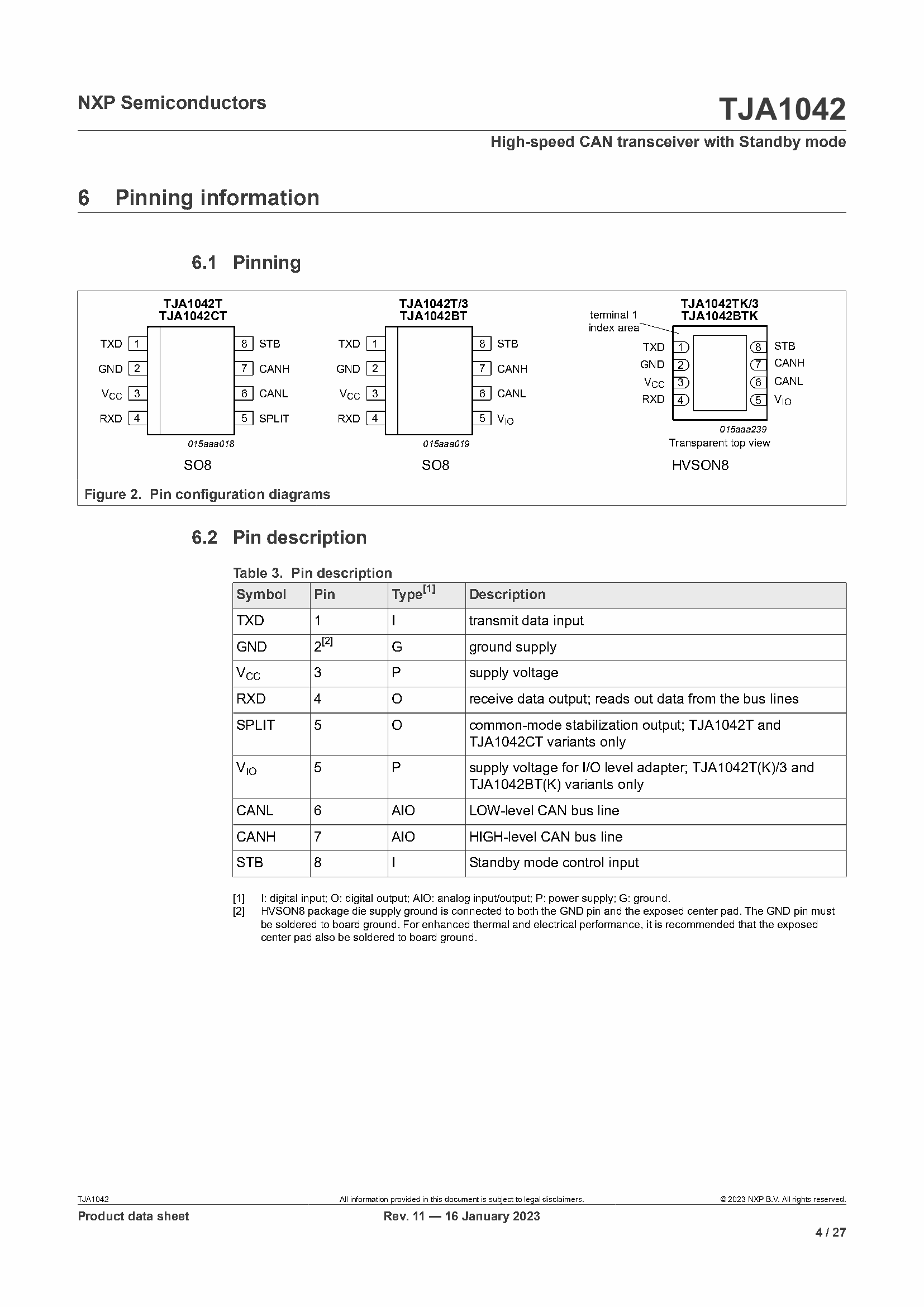
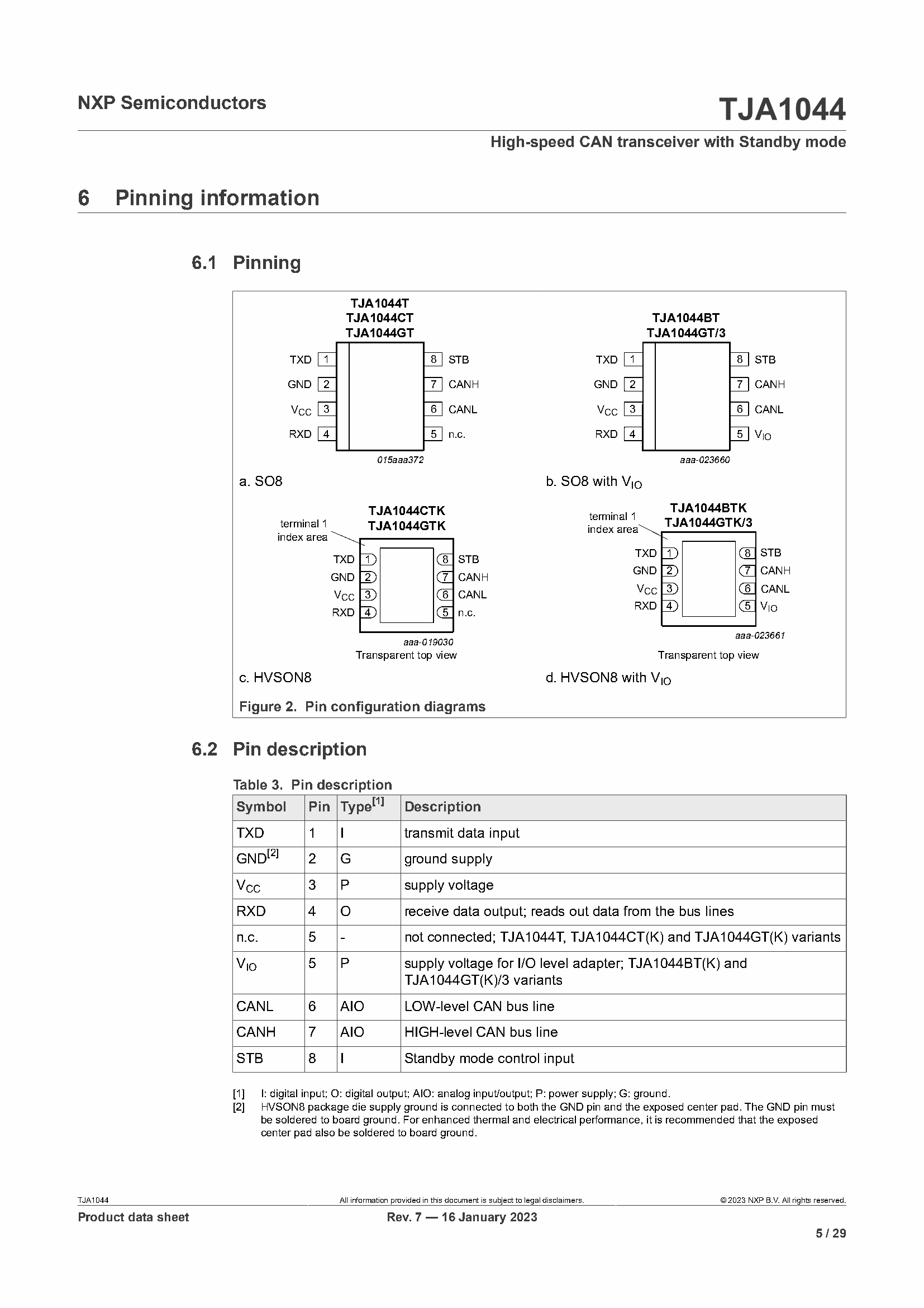
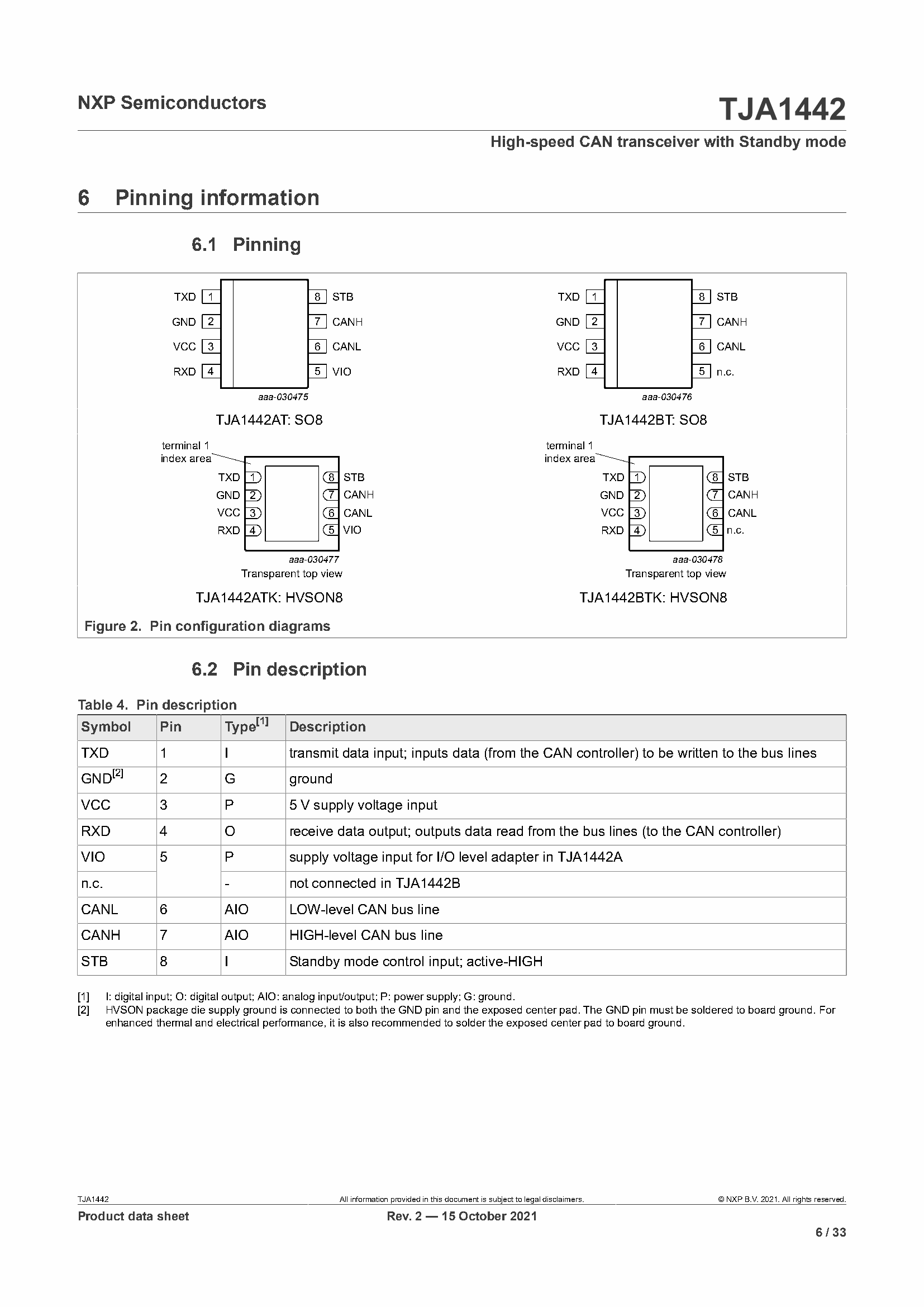
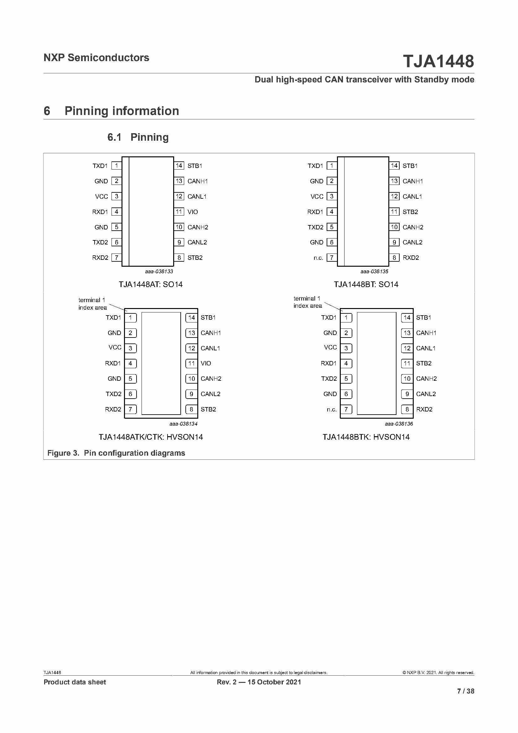
Pinning Information
Features and benefits
2.1 General
ISO 11898-2:2016 and SAE J2284-1 to SAE J2284-5 compliant
Loop delay symmetry timing enables reliable communication at data rates up to
5Mbit/s in the CAN FD fast phase
Suitable for 12V and 24V systems
Low ElectroMagnetic Emission (EME) and high ElectroMagnetic Immunity (EMI)
V input allows for direct interfacing with 3V and 5V microcontrollers
SPLIT voltage output for stabilizing the recessive bus level
Listen-only mode for node diagnosis and failure containment
Available in SO14 and HVSON14 packages
New to NXP?
Leadless HVSON14 package (3.0 mm4.5mm) with improved Automated Optical
Inspection (AOI) capability
AEC-Q100 qualified
Dark green product (halogen free and Restriction of Hazardous Substances (RoHS)
compliant)
2.2 Low-power management
Very low current Standby and Sleep modes, with local and remote wake-up
Capability to power down the entire node while supporting local, remote and host
wake-up
Wake-up source recognition
Transceiver disengages from the bus (zero load) when V absent
BAT
Functional behavior predictable under all supply conditions
2.3 Protection and diagnosis (detection and signalling)
High ESD handling capability on the bus pins
Bus pins and V protected against transients in automotive environments
BAT
Transmit Data (TXD) dominant time-out function with diagnosis
TXD-to-RXD short-circuit handler with diagnosis
Thermal protection with diagnosis
Undervoltage detection and recovery on pins V , V and V
CC IO BAT
Bus line short-circuit diagnosis
Bus dominant clamping diagnosis
Cold start diagnosis (first battery connection)
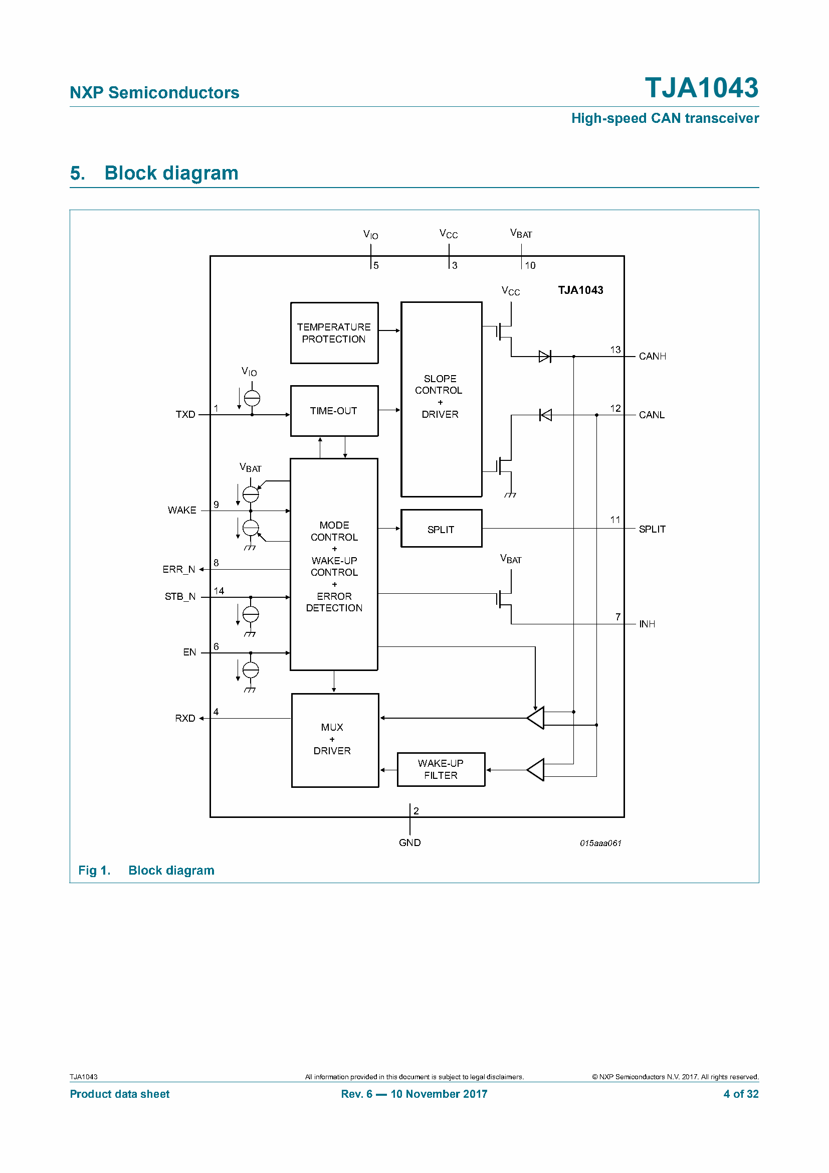
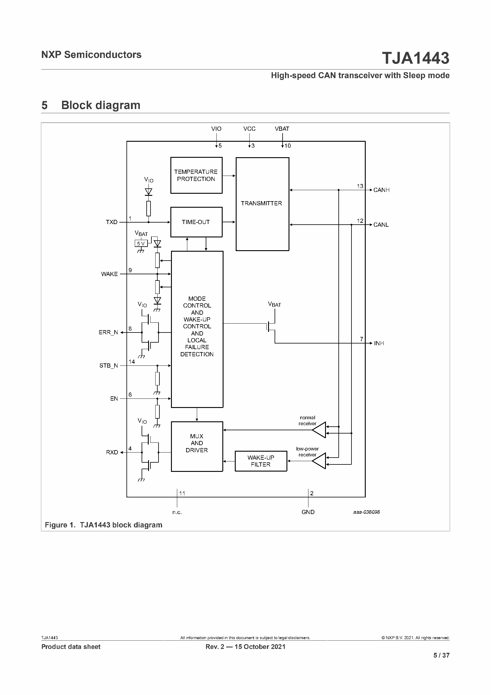
Block Digram
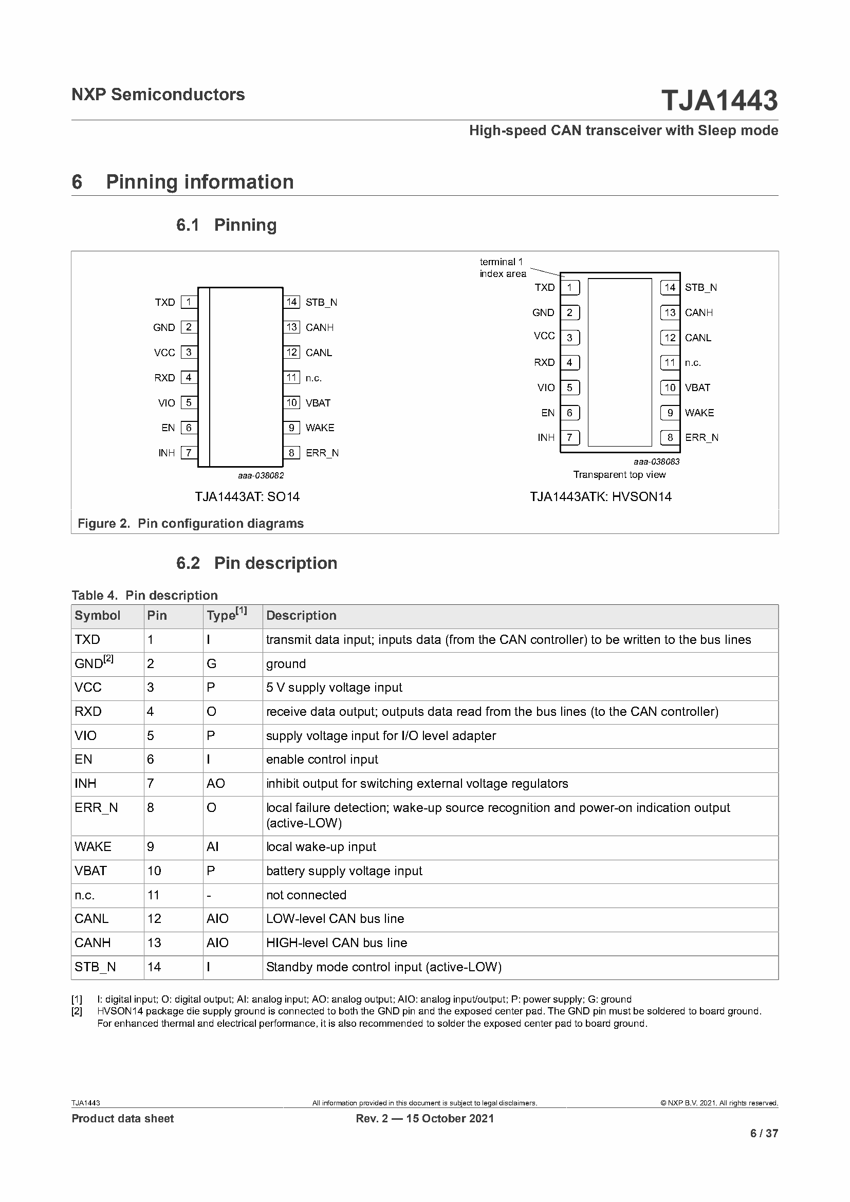
Pinning Information
Features and benefits
         2.1 General

        • Fully ISO 11898-2:2016, SAE J2284-1 to SAE J2284-5 and SAE J1939-14 compliant

        • Very low-current Standby mode with local and bus wake-up capability

        • Optimized for use in 12 V automotive systems

        • Low Electromagnetic Emission (EME) and high Electromagnetic Immunity (EMI),

        according to proposed EMC Standards IEC 62228-3 and SAE J2962-2

        • AEC-Q100 qualified

        • Dark green product (halogen free and Restriction of Hazardous Substances (RoHS)

        compliant)

        • Variants with a V pin allow for direct interfacing with 3.3 V to 5 V microcontrollers.

        Variants without a V pin can interface with 3.3 V (except TJA1044C) and 5 V-supplied

        microcontrollers, provided the microcontroller I/Os are 5 V tolerant.

        NXP Semiconductors TJA1044

        • Shorter propagation delay on the TJA1044B and TJA1044C variants supports larger

        network topologies (see Table 8)

        • Both V and non-V variants are available in SO8 and leadless HVSON8 (3.0 mm

        IO IO

        × 3.0 mm) packages; HVSON8 with improved Automated Optical Inspection (AOI)

        capability.

        2.2 Predictable and fail-safe behavior

        • Functional behavior predictable under all supply conditions

        • Transceiver disengages from the bus (high-ohmic) when the supply voltage drops

        below the switch-off undervoltage threshold

        • Transmit Data (TXD) dominant time-out functions

        • Internal biasing of TXD and STB input pins

        2.3 Low-power management

        • Very low-current Standby mode with host and bus wake-up capability

        • Variants with V pin: CAN wake-up receiver powered by V allowing V to be shut

        IO IO CC

        down

        • Variants with V pin and TJA1044C: CAN wake-up pattern filter time of 0.5 μs to

        1.8 μs, meeting Classical CAN and CAN FD requirements

        2.4 Protection

        • High ESD handling capability on the bus pins (8 kV IEC and HBM)

        • Bus pins protected against transients in automotive environments

        • Undervoltage detection on pins V and V

        CC IO

        • Thermally protected

        2.5 TJA1044 CAN FD (applicable to all product variants except

        TJA1044T)

        • Timing guaranteed for CAN FD data rates up to 5 Mbit/s

        TJA1044 All information provided in this document is subject to legal disclaimers. © 2023 NXP B.V. All rights reserved.

        Product data sheet Rev. 7 — 16 January 2023

        2 / 29

        NXP Semiconductors TJA1044
Block Digram
Pinning Information
Features and benefits
2.1 General
Fully ISO 11898-2:2016 and SAE J2284-1 to SAE J2284-5 compliant
Certified according to latest VeLIO (Vehicle LAN Interoperability and Optimization) test
requirements
Very low-current Standby mode with host and bus wake-up capability
Optimized for use in 12V automotive systems
EMC performance satisfies 'Hardware Requirements for LIN, CAN and FlexRay
Interfaces in Automotive Applications’, Version 1.3, May 2012.
AEC-Q100 qualified
Dark green product (halogen free and Restriction of Hazardous Substances (RoHS)
compliant)
TJA1044V
V input on TJA1044Vx/3 variants allows for direct interfacing with 3Vto5V
microcontrollers. Variants without a V pin can interface with 3.3V and 5V-supplied
microcontrollers, provided the microcontroller I/Os are 5 V tolerant.
Both V and non-V variants are available in SO8 and leadless HVSON8 (3.0
IO IO
mm3.0mm) packages; HVSON8 with improved Automated Optical Inspection (AOI)
capability.
2.2 Predictable and fail-safe behavior
Functional behavior predictable under all supply conditions
Transceiver disengages from bus when not powered (zero load)
Transmit Data (TXD) and bus dominant time-out functions
Internal biasing of TXD and STB input pins
2.3 Protection
High ESD handling capability on the bus pins (8 kV IEC and HBM)
Bus pins protected against transients in automotive environments
Undervoltage detection on pinsV and V
CC IO
Thermally protected
2.4 TJA1044V CAN FD
Timing guaranteed for CAN FD data rates up to 5 Mbit/s
Improved TXD to RXD propagation delay of 210 ns
TJA1044V All information provided in this document is subject to legal disclaimers. © NXP Semiconductors N.V. 2018. All rights reserved.
Product data sheet Rev. 1 — 2 March 2018 2 of 27
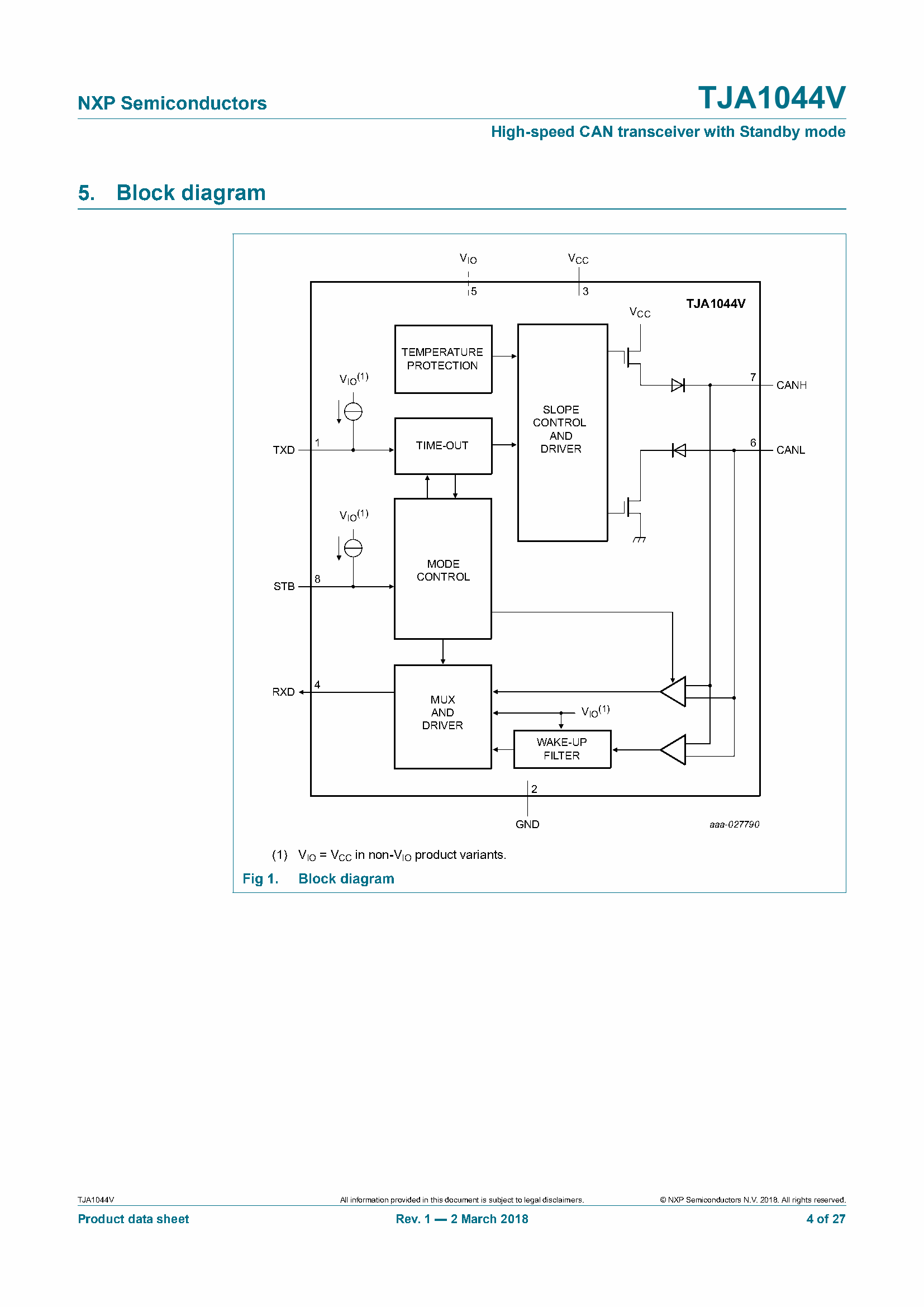
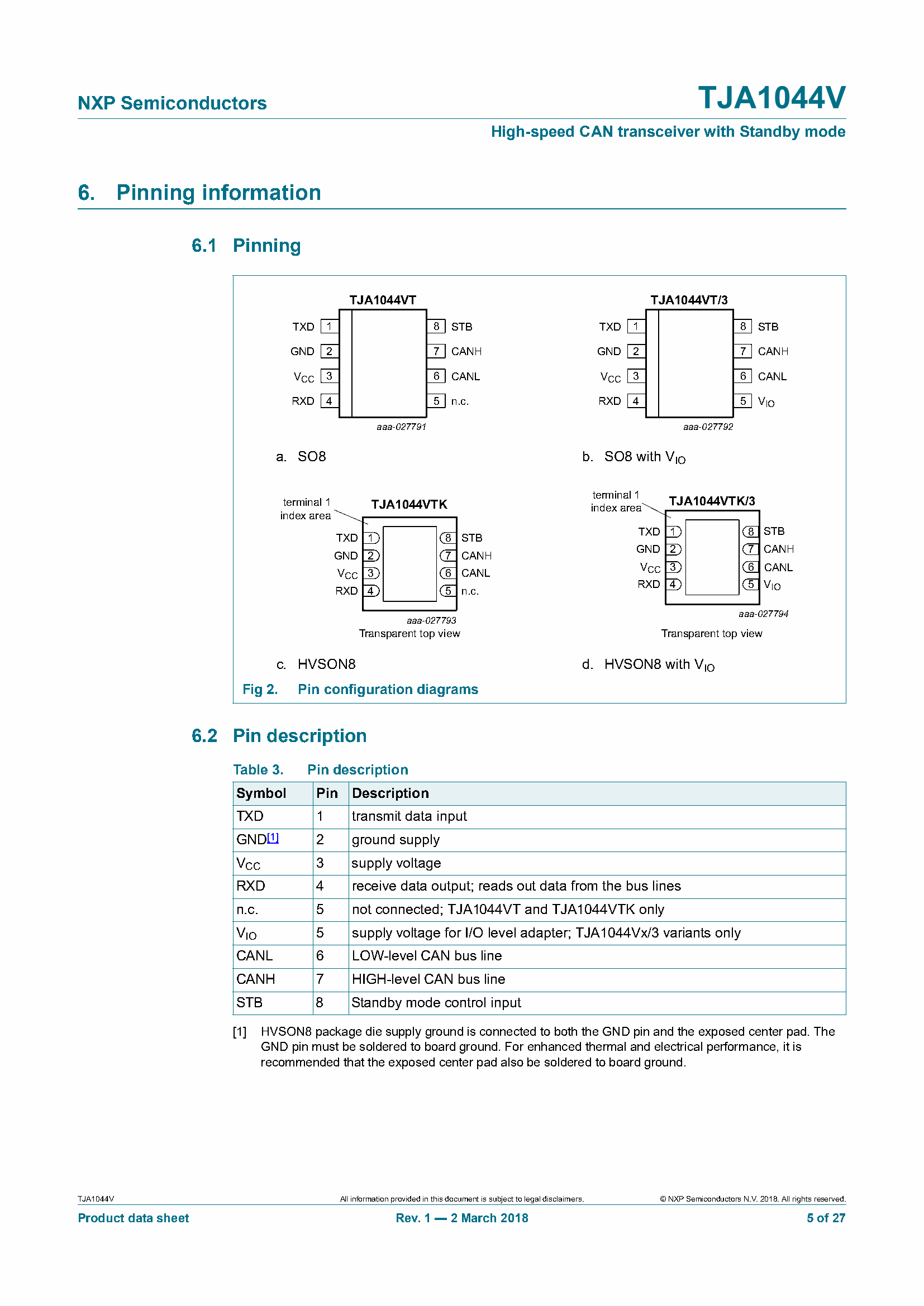
TJA1044V
Block Digram
Pinning Information
Features and benefits
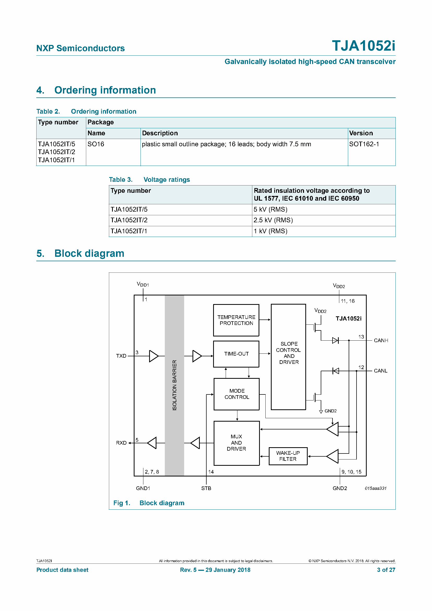
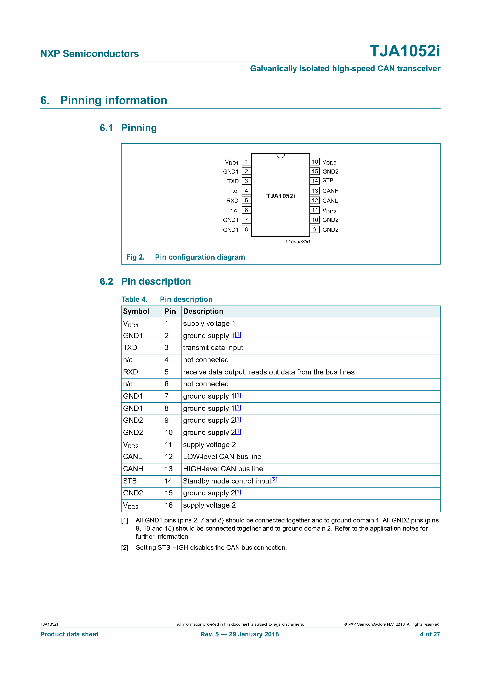
2.1 General
Isolator and Transceiver integrated into a single SO16 package, reducing board space
ISO 11898-2:2016 and SAE J2284-1 to SAE J2284-5 compliant
Timing guaranteed for data rates up to 5Mbit/s in the CAN FD fast phase
Flawless cooperation between the Isolator and the Transceiver
TJA1052i
Galvanically isolated high-speed CAN transceiver
Fewer components improves reliability in applications
Guaranteed performance (eg. max loop delay <220 ns)
Electrical transient immunity of 45 kV/s (typ)
AEC-Q100 qualified
Suitable for use in 12V and 24V systems; compatible with 3 V to 5V microcontrollers
Bus common mode voltage (V ) = 25V
cm
Low ElectroMagnetic Emission (EME) and high ElectroMagnetic Immunity (EMI)
Dark green product (halogen free and Restriction of Hazardous Substances (RoHS)
compliant)
2.2 Power management
Functional behavior predictable under all supply conditions
Transceiver disengages from the bus when not powered up (zero load)
2.3 Protection
Up to 5 kV (RMS) rated isolation
Three versions available (1 kV, 2.5 kV and 5 kV)
Voltage compliant with UL1577, IEC61010 and IEC60950
5 kV (RMS) rated isolation voltage compliant with UL1577, IEC61010 and IEC60950
Supports ISO6469 ‘Electrically propelled road vehicles. Safety specifications.’
High ESD handling capability on the bus pins
Bus pins protected against transients in automotive environments
Transmit Data (TXD) dominant time-out function
Undervoltage detection on supply pins
Block Digram
Pinning Information
Features and benefits
2.1 General
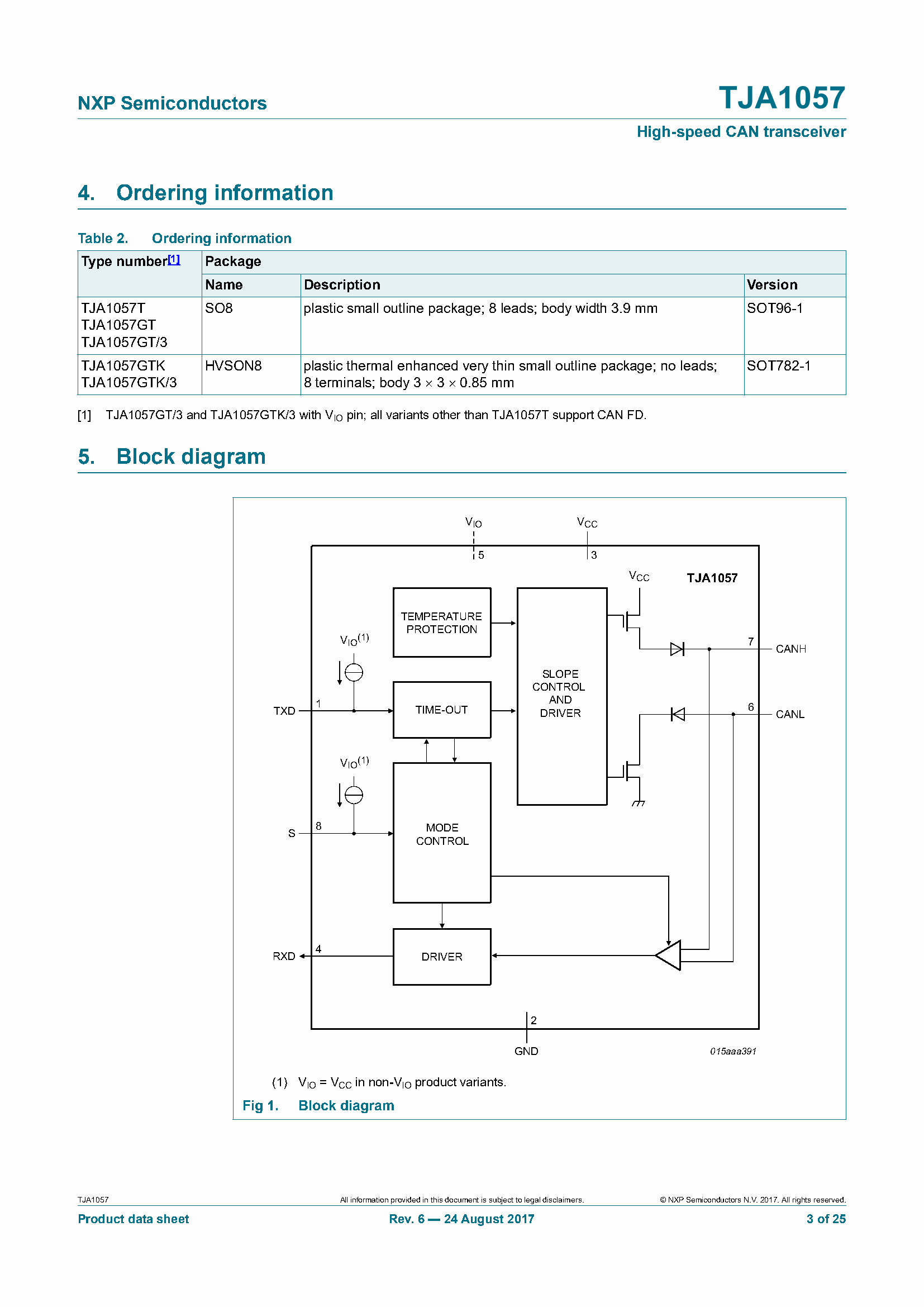
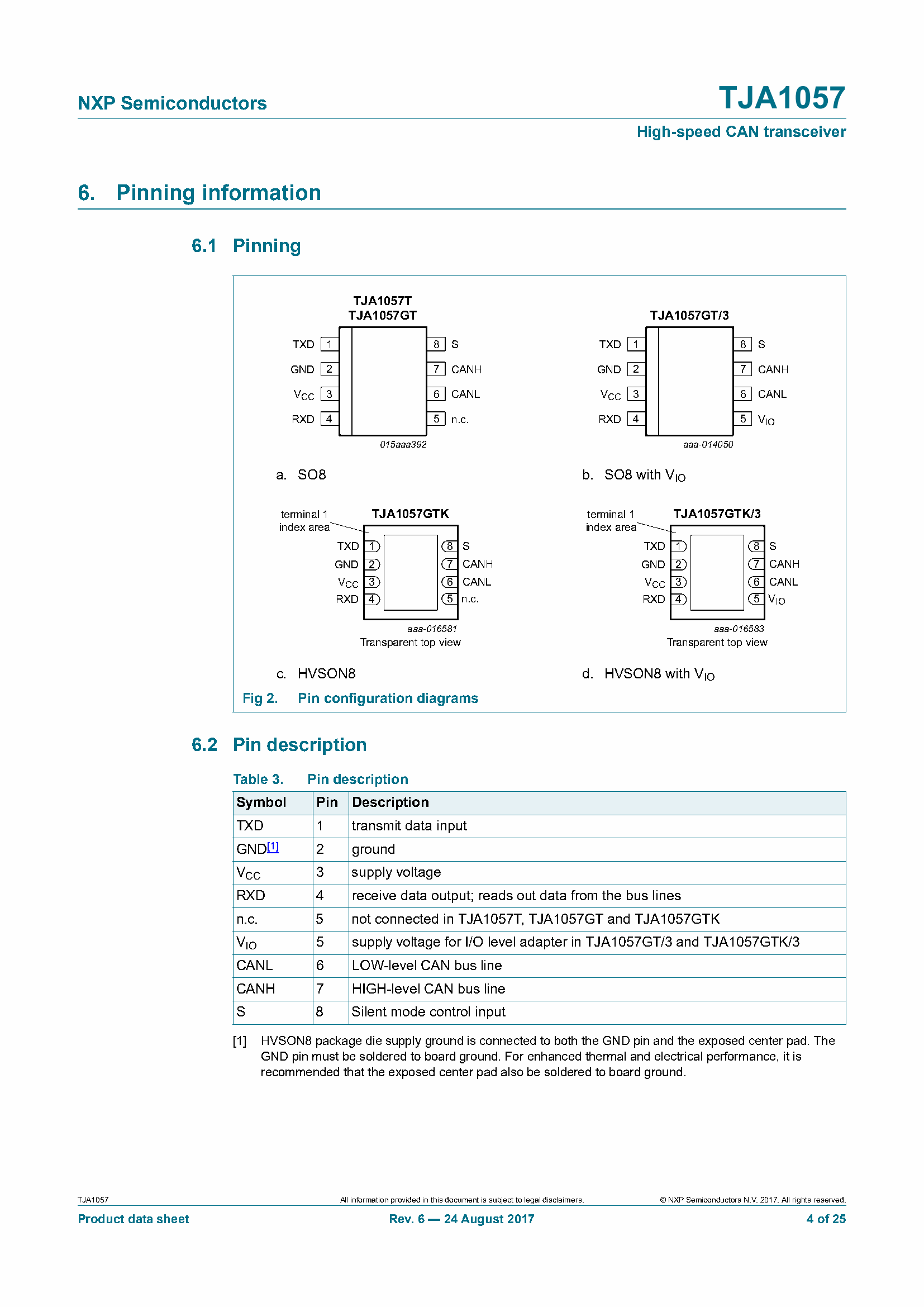
Fully ISO 11898-2:2016 and SAE J2284-1 to SAE J2284-5 compliant
Optimized for use in 12V automotive systems
EMC performance satisfies 'Hardware Requirements for LIN, CAN and FlexRay
Interfaces in Automotive Applications’, Version 1.3, May 2012.
V input on TJA1057x/3 variants allows for direct interfacing with 3Vto5V
microcontrollers. Variants without a V pin can interface with 3.3V and 5V-supplied
microcontrollers, provided the microcontroller I/Os are 5 V tolerant.
AEC-Q100 qualified
Dark green product (halogen free and Restriction of Hazardous Substances (RoHS)
compliant)
Both V and non-V variants are available in SO8 and leadless HVSON8 (3.0
IO IO
mm3.0mm) packages; HVSON8 with improved Automated Optical Inspection (AOI)
capability.
TJA1057
2.2 Predictable and fail-safe behavior
Functional behavior predictable under all supply conditions
Transceiver disengages from bus when not powered (zero load)
Transmit Data (TXD) dominant time-out function
Internal biasing of TXD and S input pins
2.3 Protection
High ESD handling capability on the bus pins (8 kV IEC and HBM)
Bus pins protected against transients in automotive environments
Undervoltage detection on pinsV and V
CC IO
Thermally protected
2.4 TJA1057 CAN FD (applicable to all product variants except TJA1057T)
Timing guaranteed for data rates up to 5 Mbit/s
Improved TXD to RXD propagation delay of 210 ns
Block Digram
Pinning Information
Features and benefits
2.1 General
ISO 11898-2:2016 and SAE J2284-1 to SAE J2284-5 compliant
Timing guaranteed for data rates up to 5Mbit/s in the CAN FD fast phase
Autonomous bus biasing
Optimized for in-vehicle high-speed CAN communication
No ‘false’ wake-ups due to CAN FD in TJA1145Ax/FD variants
High-speed CAN transceiver for partial networking
Hardware and software compatible with the TJA1145, with improved EMC
performance
2.2 Designed for automotive applications
8 kV ElectroStatic Discharge (ESD) protection, according to the Human Body Model
(HBM) on the CAN bus pins
6 kV ESD protection, according to IEC TS 62228 on pins BAT and WAKE and on the
CAN bus pins
CAN bus pins short-circuit proof to 58 V
Battery and CAN bus pins protected against transients according to ISO7637-3, test
pulses 1, 2a, 3a and 3b.
Suitable for use in 12 V and 24 V systems
Available in SO14 and leadless HVSON14 package (3 mm 4.5 mm) with improved
Automated Optical Inspection (AOI) capability
AEC-Q100 qualified
Dark green product (halogen free and Restriction of Hazardous Substances (RoHS)
compliant)
2.3 Advanced ECU power management system
Very low-current Standby and Sleep modes, with full wake-up capability
Entire node can be powered down via the inhibit output
Remote wake-up capability via standard CAN wake-up pattern or via
ISO11898-2:2016 compliant selective wake-up frame detection
Local wake-up via the WAKE pin
Wake-up source recognition
Bit rates of 50 kbit/s, 100 kbit/s, 125 kbit/s, 250 kbit/s, 500 kbit/s and 1 Mbit/s
supported during selective wake-up'
Local wake-up can be disabled to reduce current consumption
Transceiver disengages from the bus when the battery supply is removed
VIO input allows for direct interfacing with 3.3 V to 5 V microcontrollers
2.4 Protection and diagnosis
16-, 24- or 32-bit SPI for configuration, control and diagnosis
Transmit Data (TXD) dominant time-out function with diagnosis
Overtemperature warning and shut-down
Undervoltage detection and recovery on pins VCC, VIO and BAT
Cold start diagnosis (via bits PO and NMS)
Advanced system and transceiver interrupt handling
TJA1145A All information provided in this document is subject to legal disclaimers. © NXP Semiconductors N.V. 2020. All rights reserved.
Product data sheet Rev. 2 — 23 September 2020 2 of 57
High-speed CAN transceiver for partial networking
Block Digram
Pinning Information
Features and benefits
         2.1 General

        • ISO 11898-2:2016, SAE J2284-1 to SAE J2284-5 and SAE J1939-14 compliant

        • Standard CAN and CAN FD data bit rates up to 5 Mbit/s

        • Low Electromagnetic Emission (EME) and high Electromagnetic Immunity (EMI)

        • Qualified according to AEC-Q100 Grade 1

        • Silent mode for node diagnosis and failure containment

        • TJA1441A only: VIO input for interfacing with 3.3 V to 5 V microcontrollers

        • TJA1441D only: dedicated input for switching to very low-current Off mode and

        disengaging from the bus

        • All variants are available in SO8 and leadless HVSON8 (3.0 mm x 3.0 mm) packages;

        HVSON8 with improved Automated Optical Inspection (AOI) capability.

        NXP Semiconductors TJA1441

        • Dark green product (halogen free and Restriction of Hazardous Substances (RoHS)

        compliant)

        2.2 Predictable and fail-safe behavior

        • Undervoltage detection with defined handling on all supply pins

        • Full functionality guaranteed from the undervoltage detection thresholds up to the

        maximum limiting voltage values

        • Defined behavior below the undervoltage detection thresholds

        • Transceiver disengages from the bus (high-ohmic) when the supply voltage drops

        below the Off mode threshold

        • Internal biasing of TXD and mode selection input pins, to enable defined fail-safe

        behavior

        2.3 Protection

        • High ESD handling capability on the bus pins (8 kV IEC and HBM)

        • Bus pins protected against transients in automotive environments

        • Transmit Data (TXD) dominant time-out function

        • Thermally protected

        TJA1441 All information provided in this document is subject to legal disclaimers. © NXP B.V. 2021. All rights reserved.

        Product data sheet Rev. 2 — 15 October 2021

        2 / 33

        NXP Semiconductors TJA1441
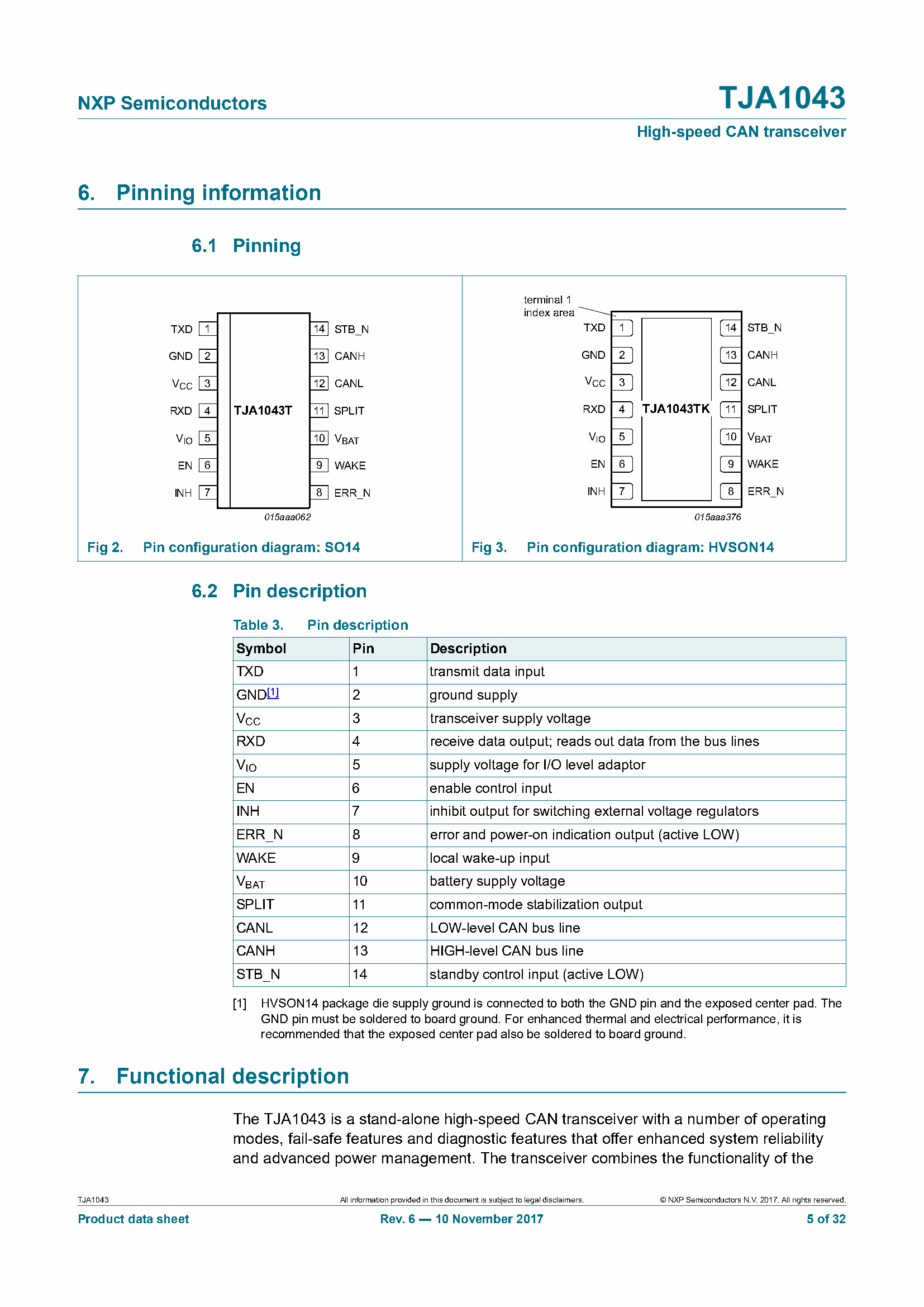
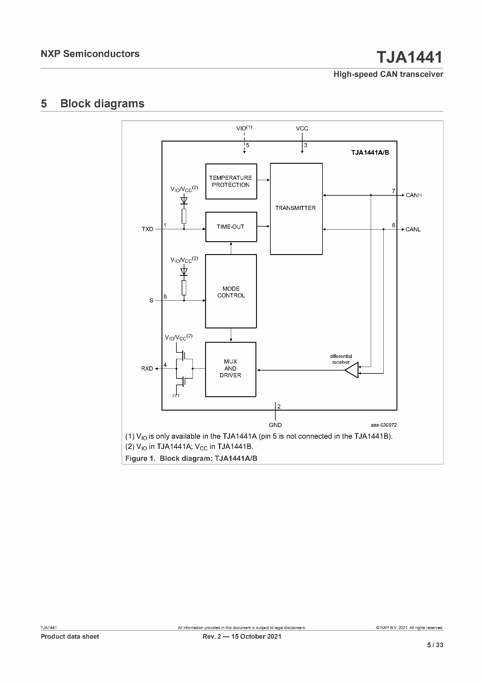
Block Digram
Pinning Information
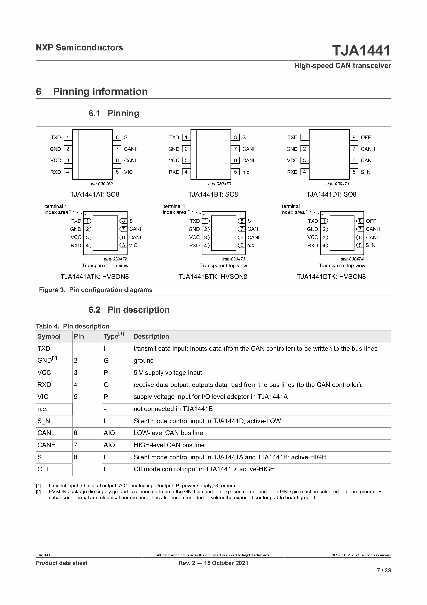
Features and benefits
         2.1 General

        • ISO 11898-2:2016, SAE J2284-1 to SAE J2284-5 and SAE J1939-14 compliant

        • Standard CAN and CAN FD data bit rates up to 5 Mbit/s

        • Low Electromagnetic Emission (EME) and high Electromagnetic Immunity (EMI)

        • Qualified according to AEC-Q100 Grade 1

        • TJA1442A only: VIO input for interfacing with 3.3 V to 5 V microcontrollers

        • All variants are available in SO8 and leadless HVSON8 (3.0 mm x 3.0 mm) packages;

        HVSON8 with improved Automated Optical Inspection (AOI) capability.

        • Dark green product (halogen free and Restriction of Hazardous Substances (RoHS)

        compliant)

        2.2 Predictable and fail-safe behavior

        • Undervoltage detection with defined handling on all supply pins

        NXP Semiconductors TJA1442

        • Full functionality guaranteed from the undervoltage detection thresholds up to the

        maximum limiting voltage values

        • Defined behavior below the undervoltage detection thresholds

        • Transceiver disengages from the bus (high-ohmic) when the supply voltage drops

        below the Off mode threshold

        • Internal biasing of TXD and mode selection input pins, to enable defined fail-safe

        behavior

        2.3 Low-power management

        • Very low-current Standby mode with host and bus wake-up capability

        • TJA1442A only: CAN wake-up receiver powered by V allowing V to be shut down

        IO CC

        • CAN wake-up pattern filter time of 0.5 μs to 1.8 μs, meeting Classical CAN and CAN

        FD requirements

        2.4 Protection

        • High ESD handling capability on the bus pins (8 kV IEC and HBM)

        • Bus pins protected against transients in automotive environments

        • Transmit Data (TXD) dominant time-out function

        • Thermally protected

        TJA1442 All information provided in this document is subject to legal disclaimers. © NXP B.V. 2021. All rights reserved.

        Product data sheet Rev. 2 — 15 October 2021

        2 / 33

        NXP Semiconductors TJA1442
Block Digram
Pinning Information
Features and benefits
         2.1 General

        • ISO 11898-2:2016, SAE J2284-1 to SAE J2284-5 and SAE J1939-14 compliant

        • Standard CAN and CAN FD data bit rates up to 5 Mbit/s

        • Low Electromagnetic Emission (EME) and high Electromagnetic Immunity (EMI)

        • Qualified according to AEC-Q100 Grade 1

        • VIO input for interfacing with 3.3 V to 5 V microcontrollers

        • Listen-only mode for node diagnosis and failure containment

        • Available in SO14 and leadless HVSON14 (3.0 mm x 4.5 mm) packages; HVSON14

        with improved Automated Optical Inspection (AOI) capability.

        • Dark green product (halogen free and Restriction of Hazardous Substances (RoHS)

        compliant)

        2.2 Predictable and fail-safe behavior

        • Undervoltage detection with defined handling on all supply pins

        • Full functionality guaranteed from the undervoltage detection thresholds up to the

        maximum limiting voltage values

        • Defined behavior below the undervoltage detection thresholds

        • Transceiver disengages from the bus (high-ohmic) when the battery voltage drops

        below the Off mode threshold

        • Internal biasing of TXD and mode selection input pins, to enable defined fail-safe

        behavior

        NXP Semiconductors TJA1443

        High-speed CAN transceiver with Sleep mode

        2.3 Low-power management

        • Very low-current Standby and Sleep modes, with host, local and bus wake-up capability

        • Entire node with TJA1443 can be powered down while still supporting local, bus and

        host wake-up

        • CAN wake-up receiver powered by V allowing V and V to be shut down

        BAT IO CC

        • CAN wake-up pattern filter time of 0.5 μs to 1.8 μs, meeting Classical CAN and CAN

        FD requirements

        2.4 Diagnosis & Protection

        • Overtemperature diagnosis

        • Transmit Data (TXD) dominant time-out and TXD-to-RXD short-circuit handler with

        diagnosis

        • Bus dominant clamping diagnosis

        • Cold start diagnosis (first battery connection)

        • High ESD handling capability on the bus pins (8 kV IEC and HBM)

        • Bus pins and VBAT protected against transients in automotive environments

        • Thermally protected

        TJA1443 All information provided in this document is subject to legal disclaimers. © NXP B.V. 2021. All rights reserved.

        2 / 37

        NXP Semiconductors TJA1443

        High-speed CAN transceiver with Sleep mode
Block Digram
Pinning Information
Features and benefits
         2.1 General

        • ISO 11898-2:2016, SAE J2284-1 to SAE J2284-5 and SAE J1939-14 compliant

        • Standard CAN and CAN FD data bit rates up to 5 Mbit/s

        • Low Electromagnetic Emission (EME) and high Electromagnetic Immunity (EMI)

        • Qualified according to AEC-Q100 Grade 1

        • TJA1448A/C only: VIO input for interfacing with 3.3 V to 5 V microcontrollers

        • Fully independent control of two transceivers combined monolithically in a single

        package

        • All variants are available in a leadless HVSON14 (3.0 mm x 4.5 mm) package with

        improved Automated Optical Inspection (AOI) capability; TJA1448A/B available in an

        SO14 package.

        NXP Semiconductors TJA1448

        Dual high-speed CAN transceiver with Standby mode

        • Dark green product (halogen free and Restriction of Hazardous Substances (RoHS)

        compliant)

        2.2 Predictable and fail-safe behavior

        • Undervoltage detection with defined handling on all supply pins

        • Full functionality guaranteed from the undervoltage detection thresholds up to the

        maximum limiting voltage values

        • Defined behavior below the undervoltage detection thresholds

        • Transceiver disengages from the bus (high-ohmic) when the supply voltage drops

        below the Off mode threshold

        • Internal biasing of TXD and mode selection input pins, to enable defined fail-safe

        behavior

        2.3 Low-power management

        • Very low-current Standby mode with host and bus wake-up capability

        • TJA1448A/C only: CAN wake-up receiver powered by V allowing V to be shut

        IO CC

        down

        • CAN wake-up pattern filter time of 0.5 μs to 1.8 μs meeting Classical CAN and CAN FD

        requirements

        • TJA1448C variant offers RXD wake-up latching to enable wake-up source readout in

        gateway applications

        2.4 Protection

        • High ESD handling capability on the bus pins (8 kV IEC and HBM)

        • Bus pins protected against transients in automotive environments

        • Transmit Data (TXD) dominant time-out function

        • Thermally protected

        TJA1448 All information provided in this document is subject to legal disclaimers. © NXP B.V. 2021. All rights reserved.

        2 / 38

        NXP Semiconductors TJA1448

        Dual high-speed CAN transceiver with Standby mode
Block Digram
Pinning Information
Features and benefits
2.1 General
• ISO 11898-2:2016, SAE J2284-1 to SAE J2284-5 and SAE J1939-14 compliant
• Implements CAN Signal Improvement Capability as defined in CiA 601-4:2019 to
significantly reduce signal ringing effects in a network
• Much tighter bit timing symmetry performance allowing more time to reduce signal
ringing
• Low Electromagnetic Emission (EME) and high Electromagnetic Immunity (EMI)
• Qualified according to AEC-Q100 Grade 1
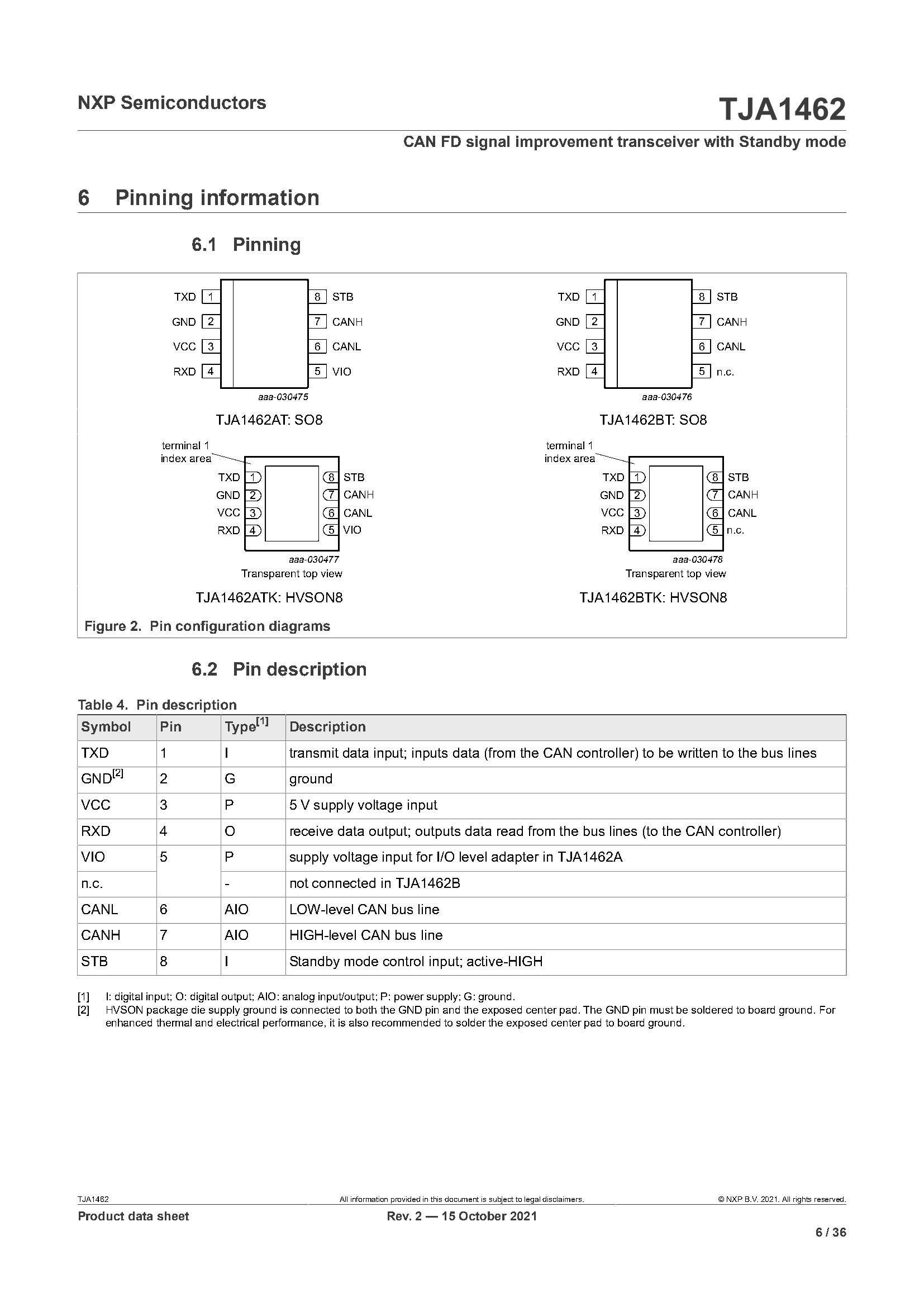
• TJA1462A only: VIO input for interfacing with 3.3 V to 5 V microcontrollers
• All variants are available in SO8 and leadless HVSON8 (3.0 mm x 3.0 mm) packages;
HVSON8 with improved Automated Optical Inspection (AOI) capability.
NXP Semiconductors TJA1462
CAN FD signal improvement transceiver with Standby mode
• Dark green product (halogen free and Restriction of Hazardous Substances (RoHS)
compliant)
2.2 Predictable and fail-safe behavior
• Undervoltage detection with defined handling on all supply pins
• Full functionality guaranteed from the undervoltage detection thresholds up to the
maximum limiting voltage values
• Defined behavior below the undervoltage detection thresholds
• Transceiver disengages from the bus (high-ohmic) when the supply voltage drops
below the Off mode threshold
• Internal biasing of TXD and mode selection input pins, to enable defined fail-safe
behavior
2.3 Low-power management
• Very low-current Standby mode with host and bus wake-up capability
• TJA1462A only: CAN wake-up receiver powered by V allowing V to be shut down
IO CC
• CAN wake-up pattern filter time of 0.5 μs to 1.8 μs, meeting Classical CAN and CAN
FD requirements
2.4 Protection
• High ESD handling capability on the bus pins (6 kV IEC and 8 kV HBM)
• Bus pins protected against transients in automotive environments
• Transmit Data (TXD) dominant time-out function
• Thermally protected
TJA1462 All information provided in this document is subject to legal disclaimers. © NXP B.V. 2021. All rights reserved.
2 / 36
NXP Semiconductors TJA1462
CAN FD signal improvement transceiver with Standby mode
Block Digram

Pinning Information
Features and benefits
         2.1 General

        • ISO 11898-2:2016, SAE J2284-1 to SAE J2284-5 and SAE J1939-14 compliant

        • Implements CAN Signal Improvement Capability as defined in CiA 601-4:2019 to

        significantly reduce signal ringing effects in a network

        • Much tighter bit timing symmetry performance allowing more time to reduce signal

        ringing

        • Low Electromagnetic Emission (EME) and high Electromagnetic Immunity (EMI)

        • Qualified according to AEC-Q100 Grade 1

        • VIO input for interfacing with 3.3 V to 5 V microcontrollers

        • Listen-only mode for node diagnosis and failure containment

        • Available in SO14 and leadless HVSON14 (3.0 mm x 4.5 mm) packages; HVSON14

        with improved Automated Optical Inspection (AOI) capability.

        • Dark green product (halogen free and Restriction of Hazardous Substances (RoHS)

        compliant)

        NXP Semiconductors TJA1463

        CAN FD signal improvement transceiver with Sleep mode

        2.2 Predictable and fail-safe behavior

        • Undervoltage detection with defined handling on all supply pins

        • Full functionality guaranteed from the undervoltage detection thresholds up to the

        maximum limiting voltage values

        • Defined behavior below the undervoltage detection thresholds

        • Transceiver disengages from the bus (high-ohmic) when the battery voltage drops

        below the Off mode threshold

        • Internal biasing of TXD and mode selection input pins, to enable defined fail-safe

        behavior

        2.3 Low-power management

        • Very low-current Standby and Sleep modes, with host, local and bus wake-up capability

        • Entire node with TJA1463 can be powered down while still supporting local, bus and

        host wake-up

        • CAN wake-up receiver powered by V allowing V and V to be shut down

        BAT IO CC

        • CAN wake-up pattern filter time of 0.5 μs to 1.8 μs, meeting Classical CAN and CAN

        FD requirements

        2.4 Diagnosis & Protection

        • Overtemperature diagnosis

        • Transmit Data (TXD) dominant time-out and TXD-to-RXD short-circuit handler with

        diagnosis

        • Bus dominant failure diagnosis

        • Cold start diagnosis (first battery connection)

        • High ESD handling capability on the bus pins (6 kV IEC and 8kV HBM)

        • Bus pins and VBAT protected against transients in automotive environments

        • Thermally protected

        TJA1463 All information provided in this document is subject to legal disclaimers. © NXP B.V. 2021. All rights reserved.

        2 / 40

        NXP Semiconductors TJA1463

        CAN FD signal improvement transceiver with Sleep mode
Block Digram

Pinning Information

