SBC
Features and benefits
         • LIN 2.0/2.1/2.2 compliant

        • SAE J2602 compliant

        • ISO 17987-4:2016 (12 V) compliant (TJA1028A/B/C/D)

        • Downward compatible with LIN 1.3

        • Internal LIN responder termination resistor

        • Voltage regulator offering 5 V or 3.3 V, 70 mA capability

        • 2 % voltage regulator accuracy over specified temperature and supply ranges

        • Voltage regulator output undervoltage detection with reset output

        • Voltage regulator is short-circuit proof to ground

        • Voltage regulator stable with ceramic, tantalum and aluminum electrolyte capacitors

        • Robust ESD performance; ±8 kV according to IEC61000-4-2 for pins LIN and V

        • Pins LIN and V protected against transients in the automotive environment (ISO

        7637)

        • Very low LIN bus leakage current of < 2 μA when battery not connected

        • LIN pin short-circuit proof to battery and ground

        • Transmit data (TXD) dominant time-out function

        • Thermally protected

        • Very low ElectroMagnetic Emission (EME)

        • High ElectroMagnetic Immunity (EMI)

        • Typical Standby mode current of 45 μA

        • Typical Sleep mode current of 12 μA

        • LIN bus wake-up function

        • K-line compatible

        • Available in SO8 and HVSON8 packages

        • Leadless HVSON8 package (3.0 mm × 3.0 mm) with improved Automated Optical

        Inspection (AOI) capability

        • Dark green product (halogen free and Restriction of Hazardous Substances (RoHS)

        compliant)
Block Digram
Pinning Information
Features and benefits
         2.1 General

        • Intended for use in road vehicles with a nominal 12 V system, full battery operating

        range from 5.0 V to 28 V

        • Very low current consumption in SLEEP and STANDBY mode

        –SLEEP mode (voltage regulator off): typically 14 µA

        –STANDBY mode (voltage regulator on): typically 22 µA

        • Remote wake-up capability via pin LIN

        • Local wake-up via pins WAKE1 and WAKE2

        –Configurable level-sensitive wake-up detection

        –Cyclic sampled wake-up detection option with synchronized bias control via pin

        HVMPO

        • Wake-up source recognition

        • Configurable high-voltage multipurpose output (HVMPO)

        –Bias control output for cyclic wake-up

        –Limp home output

        –Bias control output for battery monitoring circuit

        –General purpose input (GPI) controlled output

        • Limp home function on overtemperature, watchdog service fail, VCC undervoltage and

        RSTN short-circuit to ground

        • Overtemperature shutdown

        • Bidirectional reset pin with variable power-on reset length

        2.2 Device customization

        • Quasi one-time configuration via Serial Peripheral Interface (SPI)

        • Initial mode to configure and disable

        –Functions (e.g., LIN, watchdog, Reset, WAKE)

        –Modes (e.g., SLEEP)

        2.3 Low-dropout voltage regulator for 3.3 V/5.0 V microcontroller supply

        • 5.0 V/3.3 V nominal output voltage, ±2 % accuracy

        • 85 mA output current capability

        • Undervoltage detection with reset output

        • Excellent transient response with a small ceramic output capacitor

        • Output is short-circuit proof to GND

        2.4 LIN transceiver

        • ISO 17987-4:2016 (12 V LIN) compliant

        • LIN 2.0, LIN 2.1, LIN 2.2, LIN 2.2A compliant

        • SAE J2602-1 compliant

        • K-line compatible

        • Baud rate up to 20 kBd

        • LIN high-speed mode with fast LIN slope to support high baud rates (> 20 kBd)

        • Integrated termination resistor for LIN responder applications

        • TXD dominant time-out function

        2.5 Window watchdog

        • Watchdog with Window, Timeout and Autonomous modes

        • Microcontroller-independent clock source

        • Watchdog period selectable between 16 ms and 128 ms

        • Dedicated modes for software development and end-of-line flashing

        2.6 Designed for automotive applications

        • Qualified according to AEC-Q100

        • Load dump pulse protected against up to 43 V

        • ±8 kV Electrostatic Discharge (ESD) protection, according to the Human Body Model

        (HBM) on LIN-bus pin

        • ±6 kV ESD protection according to IEC 61000-4-2 on pins BAT, WAKE1, WAKE2 and

        ±8 kV on pin LIN

        • Bus terminal and battery pin protected against transients in the automotive environment

        (ISO 7637)

        • LIN-bus pin short-circuit proof to battery and ground

        • Leadless HVSON14 package (3.0 mm × 4.5 mm) supporting Automated Optical

        Inspection (AOI) capability and low thermal resistance

        2 / 42
Block Digram
Pinning Information
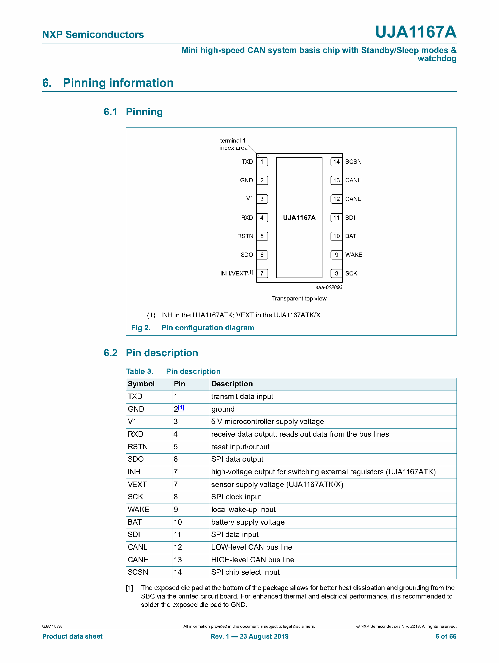
Pinning Information
Features and benefits
2.1 General
ISO 11898-2:2016 and SAE J2284-1 to SAE J2284-5 compliant high-speed CAN
transceiver
Hardware and software compatible with the UJA116x product family and with improved
EMC performance
Loop delay symmetry timing enables reliable communication at data rates up to
5Mbit/s in the CAN FD fast phase
Autonomous bus biasing according to ISO 11898-6
Fully integrated 5 V/100 mA low-drop voltage regulator for 5V microcontroller
supply(V1)
Bus connections are truly floating when power to pin BAT is off
2.2 Designed for automotive applications
8 kV ElectroStatic Discharge (ESD) protection, according to the Human Body Model
(HBM) on the CAN bus pins
6 kV ESD protection, according to IEC TS 62228 on the CAN bus pins and on pin
CAN bus pins short-circuit proof to 58 V
Battery and CAN bus pins protected against automotive transients according to
ISO7637-3
Very low quiescent current in Standby mode with full wake-up capability
Leadless HVSON14 package (3.0 mm 4.5 mm) with improved Automated Optical
Inspection (AOI) capability and low thermal resistance
Dark green product (halogen free and Restriction of Hazardous Substances (RoHS)
compliant)
NXP Semiconductors
Mini high-speed CAN system basis chip with Standby mode
2.3 Low-drop voltage regulator for 5 V microcontroller supply (V1)
5 V nominal output; 2 % accuracy
100 mA output current capability
Current limiting above 150 mA
On-resistance of 5 (max)
Support for microcontroller RAM retention down to a battery voltage of 2 V
Undervoltage reset at 90 % of nominal value
Excellent transient response with a 4.7 F ceramic output capacitor
Short-circuit to GND/overload protection on pin V1
2.4 Power Management
Standby mode featuring very low supply current; voltage V1 remains active to maintain
the supply to the microcontroller
Remote wake-up capability via standard CAN wake-up pattern
2.5 System control and diagnostic features
Mode control via pin STBN
Overtemperature shutdown
Bidirectional reset pin
Block Digram
Pinning Information

Features and benefits
2.1 General
ISO 11898-2:2016 and SAE J2284-1 to SAE J2284-5 compliant high-speed CAN
transceiver
Hardware and software compatible with the UJA116x product family and with improved
EMC performance
Loop delay symmetry timing enables reliable communication at data rates up to
5Mbit/s in the CAN FD fast phase
Autonomous bus biasing according to ISO 11898-6
Fully integrated 5 V/100 mA low-drop voltage regulator for 5V microcontroller
supply(V1)
Bus connections are truly floating when power to pin BAT is off
2.2 Designed for automotive applications
8 kV ElectroStatic Discharge (ESD) protection, according to the Human Body Model
(HBM) on the CAN bus pins
6 kV ESD protection, according to IEC TS 62228 on the CAN bus pins and on pin
CAN bus pins short-circuit proof to 58 V
Battery and CAN bus pins protected against automotive transients according to
ISO7637-3
Very low quiescent current in Standby mode with full wake-up capability
Leadless HVSON14 package (3.0 mm 4.5 mm) with improved Automated Optical
Inspection (AOI) capability and low thermal resistance
Dark green product (halogen free and Restriction of Hazardous Substances (RoHS)
compliant)
2.3 Low-drop voltage regulator for 5 V microcontroller supply (V1)
5 V nominal output; 2 % accuracy
100 mA output current capability
Current limiting above 150 mA
On-resistance of 5 (max)
Support for microcontroller RAM retention down to a battery voltage of 2 V
Undervoltage reset with selectable detection thresholds: 60 %, 70 %, 80 % or 90 % of
output voltage
Excellent transient response with a 4.7 F ceramic output capacitor
Short-circuit to GND/overload protection on pin V1
2.4 Power Management
Standby mode featuring very low supply current; voltage V1 remains active to maintain
the supply to the microcontroller
Remote wake-up capability via standard CAN wake-up pattern
Wake-up source recognition
Remote wake-up can be disabled to reduce current consumption
2.5 System control and diagnostic features
Mode control via the Serial Peripheral Interface (SPI)
Overtemperature warning and shutdown
Watchdog with independent clock source
Watchdog can be operated in Window, Timeout and Autonomous modes
Optional cyclic wake-up in watchdog Timeout mode
Watchdog automatically re-enabled when wake-up event captured
Watchdog period selectable between 8 ms and 4 s
Supports remote flash programming via the CAN bus
16-, 24- and 32-bit SPI for configuration, control and diagnosis
Bidirectional reset pin with variable power-on reset length to support a variety of
microcontrollers
Configuration of selected functions via non-volatile memory
Block Digram
Pinning Information
Features and benefits
2.1 General
ISO 11898-2:2016 and SAE J2284-1 to SAE J2284-5 compliant high-speed CAN
transceiver
Hardware and software compatible with the UJA116x product family and with improved
EMC performance
Loop delay symmetry timing enables reliable communication at data rates up to
5Mbit/s in the CAN FD fast phase
Autonomous bus biasing according to ISO 11898-6
Fully integrated 5 V/100 mA low-drop voltage regulator for 5V microcontroller
supply(V1)
Bus connections are truly floating when power to pin BAT is off
2.2 Designed for automotive applications
8 kV ElectroStatic Discharge (ESD) protection, according to the Human Body Model
(HBM) on the CAN bus pins
6 kV ESD protection, according to IEC TS 62228 on the CAN bus pins, the sensor
supply output VEXT and on pins BAT and WAKE
CAN bus pins short-circuit proof to 58 V
Battery and CAN bus pins protected against automotive transients according to
ISO7637-3
Very low quiescent current in Standby and Sleep modes with full wake-up capability
Leadless HVSON14 package (3.0 mm 4.5 mm) with improved Automated Optical
Inspection (AOI) capability and low thermal resistance
Dark green product (halogen free and Restriction of Hazardous Substances (RoHS)
compliant)
2.3 Low-drop voltage regulator for 5 V microcontroller supply (V1)
5 V nominal output; 2 % accuracy
100 mA output current capability
Current limiting above 150 mA
On-resistance of 5 (max)
Support for microcontroller RAM retention down to a battery voltage of 2 V
Undervoltage reset with selectable detection thresholds: 60 %, 70 %, 80 % or 90 % of
output voltage
Excellent transient response with a 4.7 F ceramic output capacitor
Short-circuit to GND/overload protection on pin V1
Turned off in Sleep mode
2.4 Power Management
Standby mode featuring very low supply current; voltage V1 remains active to maintain
the supply to the microcontroller
Sleep mode featuring very low supply current with voltage V1 switched off
Remote wake-up capability via standard CAN wake-up pattern
Local wake-up via the WAKE pin
Wake-up source recognition
Local and/or remote wake-up can be disabled to reduce current consumption
High-voltage output (INH) for controlling an external voltage (UJA1167ATK)
2.5 System control and diagnostic features
Mode control via the Serial Peripheral Interface (SPI)
Overtemperature warning and shutdown
Watchdog with independent clock source
Watchdog can be operated in Window, Timeout and Autonomous modes
Optional cyclic wake-up in watchdog Timeout mode
Watchdog automatically re-enabled when wake-up event captured
Watchdog period selectable between 8 ms and 4 s
Supports remote flash programming via the CAN bus
16-, 24- and 32-bit SPI for configuration, control and diagnosis
Bidirectional reset pin with variable power-on reset length to support a variety of
microcontrollers
Configuration of selected functions via non-volatile memory
Product data sheet Rev. 1 — 23 August 2019 2 of 66
2.6 Sensor supply voltage (pin VEXT of UJA1167ATK/X)
5 V nominal output; 2 % accuracy
30 mA output current capability
Current limiting above 30 mA
Excellent transient response with a 4.7 F ceramic output load capacitor
Protected against short-circuits to GND and to the battery
High ESD robustness of 6 kV according to IEC TS 62228
Can handle negative voltages as low as 18 V
Product data sheet Rev. 1 — 23 August 2019 3 of 66
3. Product family overview
Table 1. Feature over view of UJA1167A SBC family
Modes Supplies Host Interface Additional Features
Device
UJA1167ATK ● ● ● ● ● ● ● ● ● ●
UJA1167ATK/X ● ● ● ● ● ● ● ● ● ●
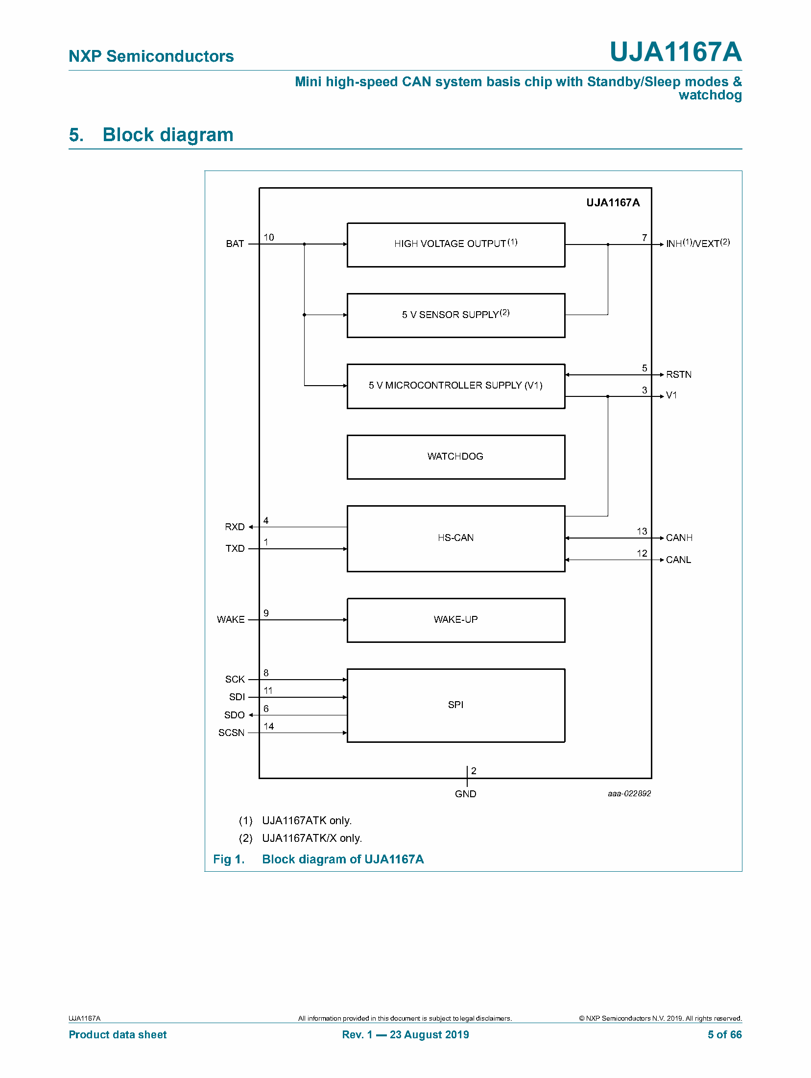
Block Digram
Pinning Information
Features and benefits
2.1 General
ISO 11898-2:2016 and SAE J2284-1 to SAE J2284-5 compliant high-speed CAN
transceiver
Hardware and software compatible with the UJA116x product family and with improved
EMC performance
Loop delay symmetry timing enables reliable communication at data rates up to
5Mbit/s in the CAN FD fast phase
Autonomous bus biasing according to ISO 11898-6
Fully integrated 5 V/100 mA low-drop voltage regulator for 5V microcontroller
supply(V1)
Bus connections are truly floating when power to pin BAT is off
No ‘false’ wake-ups due to CAN FD frame detection in UJA1168ATK/F and
UJA1168ATK/XF
2.2 Designed for automotive applications
8 kV ElectroStatic Discharge (ESD) protection, according to the Human Body Model
(HBM) on the CAN bus pins
6 kV ESD protection, according to IEC TS 62228 on the CAN bus pins, the sensor
supply output VEXT and on pins BAT and WAKE
CAN bus pins short-circuit proof to 58 V
Battery and CAN bus pins protected against automotive transients according to
ISO7637-3
Very low quiescent current in Standby and Sleep modes with full wake-up capability
Leadless HVSON14 package (3.0 mm 4.5 mm) with improved Automated Optical
Inspection (AOI) capability and low thermal resistance
Dark green product (halogen free and Restriction of Hazardous Substances (RoHS)
compliant)
2.3 Low-drop voltage regulator for 5 V microcontroller supply (V1)
5 V nominal output; 2 % accuracy
100 mA output current capability
Current limiting above 150 mA
On-resistance of 5 (max)
Support for microcontroller RAM retention down to a battery voltage of 2 V
Undervoltage reset with selectable detection thresholds: 60 %, 70 %, 80 % or 90 % of
output voltage
Excellent transient response with a 4.7 F ceramic output capacitor
Short-circuit to GND/overload protection on pin V1
Turned off in Sleep mode
2.4 Power Management
Standby mode featuring very low supply current; voltage V1 remains active to maintain
the supply to the microcontroller
Sleep mode featuring very low supply current with voltage V1 switched off
Remote wake-up capability via standard CAN wake-up pattern or via ISO11898-6
compliant selective wake-up frame detection, including CAN FD-passive support in /F
and /XF variants
Bit rates of 50kbit/s, 100kbit/s, 125kbit/s, 250kbit/s, 500kbit/s and 1Mbit/s
supported during selective wake-up
Local wake-up via the WAKE pin
Wake-up source recognition
Local and/or remote wake-up can be disabled to reduce current consumption
High-voltage output (INH) for controlling an external voltage (UJA1168ATK and
UJA1168ATK/F)
UJA1168A All information provided in this document is subject to legal disclaimers. © NXP Semiconductors N.V. 2019. All rights reserved.
Product data sheet Rev. 1 — 23 August 2019 2 of 74
2.5 System control and diagnostic features
Mode control via the Serial Peripheral Interface (SPI)
Overtemperature warning and shutdown
Watchdog with independent clock source
Watchdog can be operated in Window, Timeout and Autonomous modes
Optional cyclic wake-up in watchdog Timeout mode
Watchdog automatically re-enabled when wake-up event captured
Watchdog period selectable between 8 ms and 4 s
Supports remote flash programming via the CAN bus
16-, 24- and 32-bit SPI for configuration, control and diagnosis
Bidirectional reset pin with variable power-on reset length to support a variety of
microcontrollers
Configuration of selected functions via non-volatile memory
2.6 Sensor supply voltage (pin VEXT of UJA1168ATK/X and
UJA1168ATK/XF)
5 V nominal output; 2 % accuracy
30 mA output current capability
Current limiting above 30 mA
Excellent transient response with a 4.7 F ceramic output load capacitor
Protected against short-circuits to GND and to the battery
High ESD robustness of 6 kV according to IEC TS 62228
Can handle negative voltages as low as 18 V
UJA1168A All information provided in this document is subject to legal disclaimers. © NXP Semiconductors N.V. 2019. All rights reserved.
Product data sheet Rev. 1 — 23 August 2019 3 of 74
3. Product family overview
Table 1. Feature over view of UJA1168A SBC family
Modes Supplies Host Additional Features
Interface
Device
UJA1168ATK ● ● ● ● ● ● ● ● ● ● ●
UJA1168ATK/X ● ● ● ● ● ● ● ● ● ● ●
UJA1168ATK/F ● ● ● ● ● ● ● ● ● ● ● ●
UJA1168ATK/XF ● ● ● ● ● ● ● ● ● ● ● ●
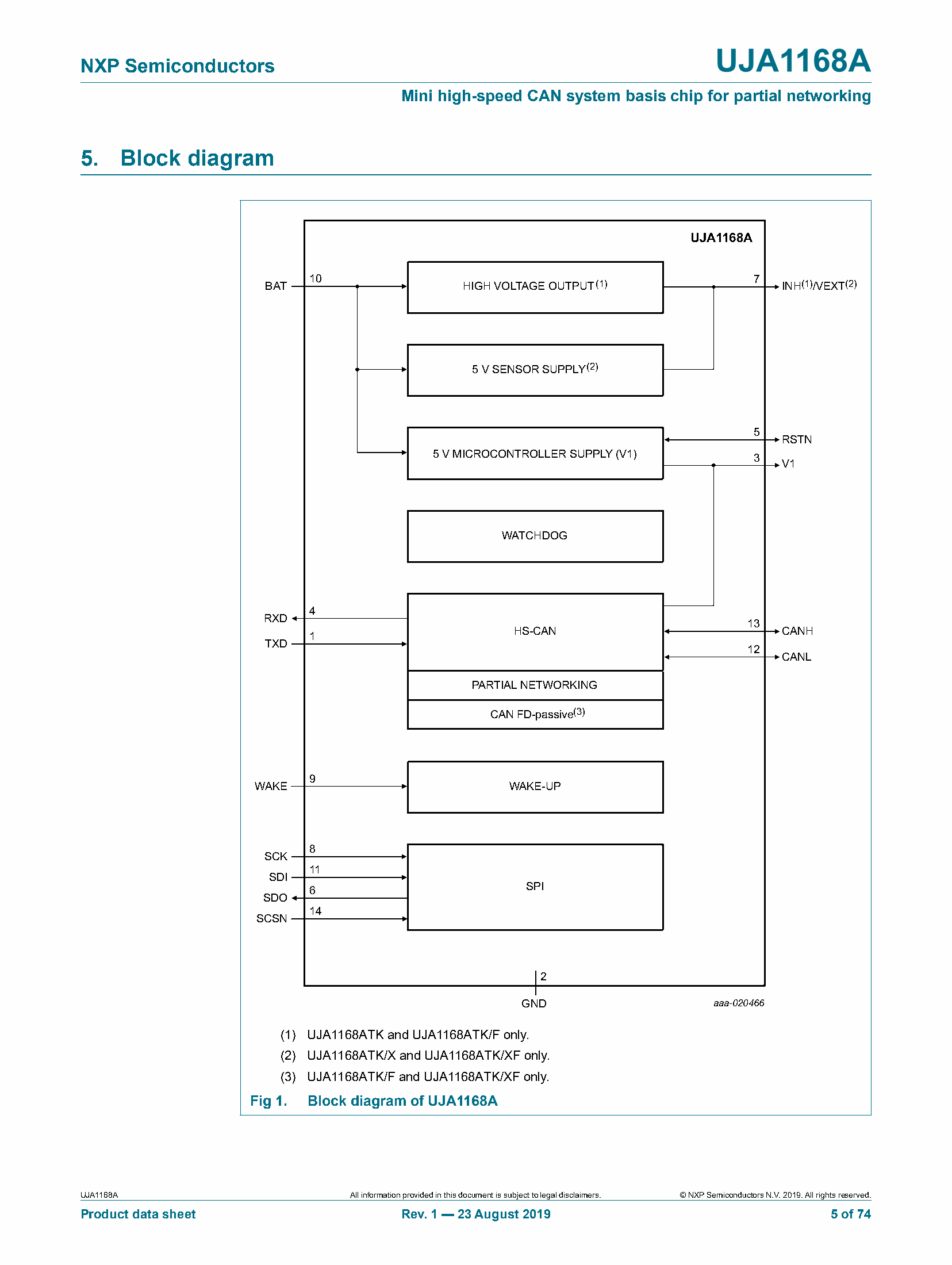
Block Digram
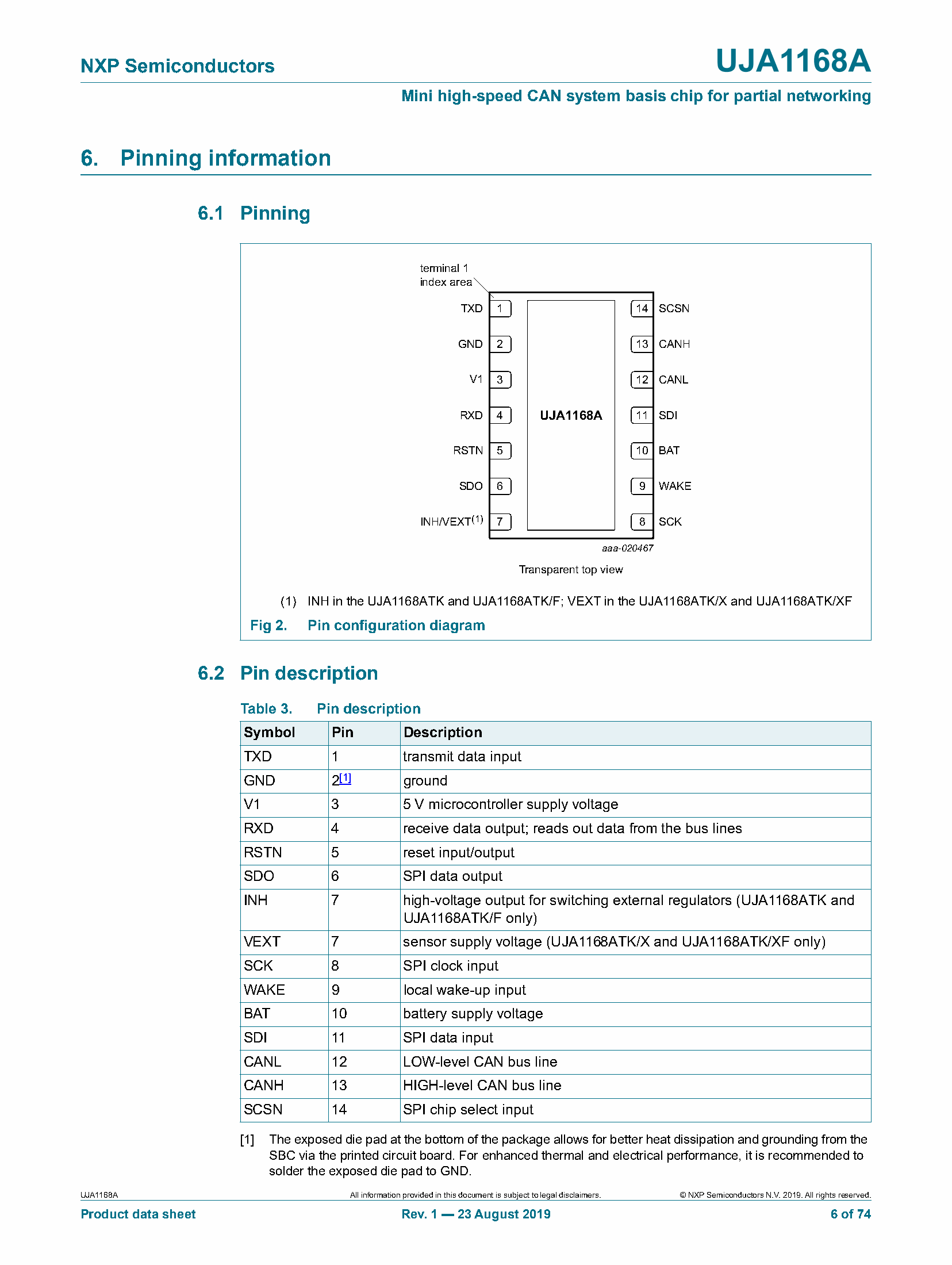
Pinning Information
Features and benefits
2.1 General
ISO11898-2:201x (upcoming merged ISO11898-2/5/6) compliant 1Mbit/s high-speed
CAN transceiver supporting CAN FD active communication up to 2Mbit/s in the CAN
FD data field (all six variants)
Autonomous bus biasing according to ISO11898-6:2013 and ISO11898-2:201x
Scalable 5V or 3.3V 250mA low-drop voltage regulator for 5 V/3.3V microcontroller
supply (V1) based on external PNP transistor concept for thermal scaling
CAN-bus connections are truly floating when power to pin BAT is off
No ‘false’ wake-ups due to CAN FD traffic (in variants supporting partial networking)
2.2 Designed for automotive applications
8 kV ElectroStatic Discharge (ESD) protection, according to the Human Body Model
(HBM) on the CAN-bus pins
6 kV ESD protection according to IEC 61000-4-2 on pins BAT, WAKE, VEXT and the
CAN-bus pins
CAN-bus pins short-circuit proof to 58 V
Battery and CAN-bus pins protected against automotive transients according to
ISO7637-3
Very low quiescent current in Standby and Sleep modes with full wake-up capability
Leadless HVSON20 package (3.5 mm 5.5 mm) with improved Automated Optical
Inspection (AOI) capability and low thermal resistance
Dark green product (halogen free and Restriction of Hazardous Substances (RoHS)
compliant)
2.3 Low-drop voltage regulator for 5 V/3.3 V microcontroller supply (V1)
5 V/3.3V nominal output; 2% accuracy
250 mA output current capability
Thermal management via optional external PNP
Current limiting above 250 mA
Support for microcontroller RAM retention down to a battery voltage of 2 V (5V only)
Undervoltage reset with selectable detection thresholds of 60%, 70%, 80% or 90%
of output voltage, configurable in non-volatile memory (5V variants only)
Excellent transient response with a small ceramic output capacitor
Output is short-circuit proof to GND
Turned off in Sleep mode
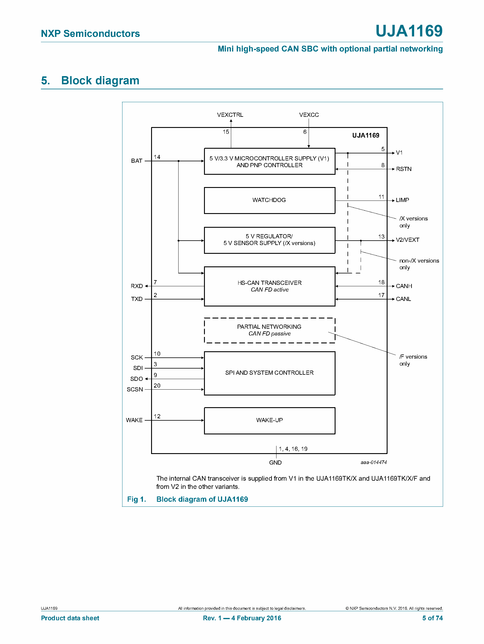
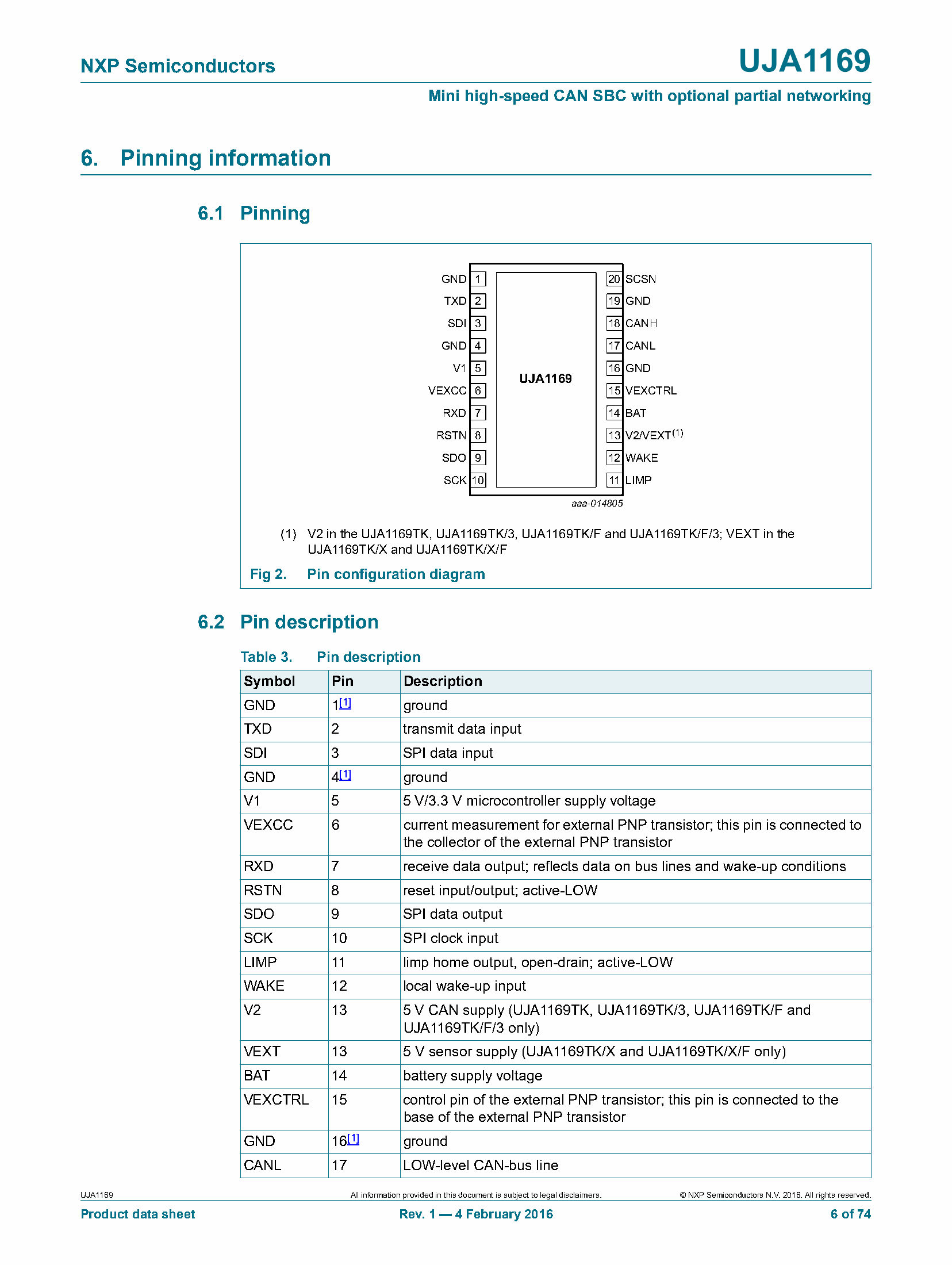
2.4 On-board CAN supply (V2; UJA1169TK, UJA1169TK/F, UJA1169TK/3
and UJA1169TK/F/3 only)
5 V nominal output; 2% accuracy
100 mA output current capability
Current limiting above 100mA
Excellent transient response with a small ceramic output capacitor
UJA1169 All information provided in this document is subject to legal disclaimers. © NXP Semiconductors N.V. 2016. All rights reserved.
Product data sheet Rev. 1 — 4 February 2016 2 of 74
UJA1169
Mini high-speed CAN SBC with optional partial networking
Output is short-circuit proof to GND
User-defined on/off behavior via SPI
2.5 Off-board sensor supply (VEXT; UJA1169TK/X and UJA1169TK/X/F
only)
5 V nominal output; 2% accuracy
100 mA output current capability
Current limiting above 100 mA
Excellent transient response with a small ceramic output load capacitor
Output is short-circuit proof to BAT, GND and negative voltages down to 18V
User-defined on/off behavior via SPI
2.6 Power Management
Standby mode featuring very low supply current; voltage V1 remains active to maintain
the supply to the microcontroller
Sleep mode featuring very low supply current with voltage V1 switched off
Remote wake-up capability via standard CAN wake-up pattern or ISO11898-6:2013
and ISO11898-2:201x compliant selective wake-up frame detection including CAN FD
passive support (/F versions only)
Local wake-up via the WAKE pin
Wake-up source recognition
2.7 System control and diagnostic features
Mode control via the Serial Peripheral Interface (SPI)
Overtemperature warning and shutdown
Watchdog with Window, Timeout and Autonomous modes and microcontroller-
independent clock source
Optional cyclic wake-up in watchdog Timeout mode
Watchdog automatically re-enabled when wake-up event captured
Watchdog period selectable between 8 ms and 4 s supporting remote flash
programming via the CAN-bus
LIMP output pin with configurable activation threshold
Watchdog failure, RSTN clamping and overtemperature events trigger the dedicated
LIMP output signal
16-, 24- and 32-bit SPI for configuration, control and diagnosis
Bidirectional reset pin with variable power-on reset length; configurable in non-volatile
memory to support a number of different microcontrollers
Customer configuration of selected functions via non-volatile memory
Dedicated modes for software development and end-of-line flashing
UJA1169 All information provided in this document is subject to legal disclaimers. © NXP Semiconductors N.V. 2016. All rights reserved.
Product data sheet Rev. 1 — 4 February 2016 3 of 74
UJA1169
Mini high-speed CAN SBC with optional partial networking
3. Product family overview
Table 1. Feature over view of UJA1169 SBC family
Modes Supplies Host Additional Features
Interface
Device
UJA1169TK ● ● ● ● ● ● ● ● ● ● ●
UJA1169TK/X ● ● ● ● ● ● ● ● ● ● ●
UJA1169TK/F ● ● ● ● ● ● ● ● ● ● ● ● ●
UJA1169TK/X/F ● ● ● ● ● ● ● ● ● ● ● ● ●
UJA1169TK/3 ● ● ● ● ● ● ● ● ● ● ●
UJA1169TK/F/3 ● ● ● ● ● ● ● ● ● ● ● ● ●
Block Digram
Pinning Information
Features and benefits
2.1 General
ISO11898-2:2016 and SAE J2284-1 to SAE J2284-5 compliant high-speed CAN
transceiver supporting CAN FD active communication up to 5Mbit/s in the CAN FD
data field (all six variants)
Autonomous bus biasing according to ISO11898-2:2016
Scalable 5V or 3.3V 250mA low-drop voltage regulator for 5 V/3.3V microcontroller
supply (V1) based on external PNP transistor concept for thermal scaling
CAN-bus connections are truly floating when power to pin BAT is off
No ‘false’ wake-ups due to CAN FD traffic (in variants supporting partial networking)
Hardware and software compatible with the UJA1169 product family
2.2 Designed for automotive applications
8 kV ElectroStatic Discharge (ESD) protection, according to the Human Body Model
(HBM) on the CAN-bus pins
6 kV ESD protection according to IEC TS 62228 on pins BAT, WAKE, VEXT and the
CAN-bus pins
CAN-bus pins short-circuit proof to 58 V
Battery and CAN-bus pins protected against automotive transients according to
ISO7637-3
Very low quiescent current in Standby and Sleep modes with full wake-up capability
Leadless HVSON20 package (3.5 mm 5.5 mm) with improved Automated Optical
Inspection (AOI) capability and low thermal resistance
Dark green product (halogen free and Restriction of Hazardous Substances (RoHS)
compliant)
2.3 Low-drop voltage regulator for 5 V/3.3 V microcontroller supply (V1)
5 V/3.3V nominal output; 2% accuracy
250 mA output current capability
Thermal management via optional external PNP
Current limiting above 250 mA
Support for microcontroller RAM retention down to a battery voltage of 2 V (5V
variants only)
Undervoltage reset with selectable detection thresholds of 60%, 70%, 80% or 90%
of output voltage, configurable in non-volatile memory (5V variants only)
Excellent transient response with a small ceramic output capacitor
Output is short-circuit proof to GND
Turned off in Sleep mode
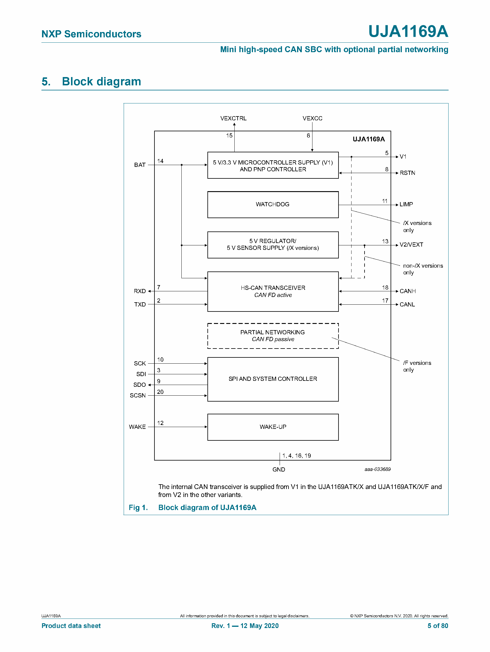
2.4 On-board CAN supply (V2; UJA1169ATK, UJA1169ATK/F,
UJA1169ATK/3 and UJA1169ATK/F/3 only)
5 V nominal output; 2% accuracy
100 mA output current capability
UJA1169A All information provided in this document is subject to legal disclaimers. © NXP Semiconductors N.V. 2020. All rights reserved.
Product data sheet Rev. 1 — 12 May 2020 2 of 80
UJA1169A
Current limiting above 100mA
Excellent transient response with a small ceramic output capacitor
Output is short-circuit proof to GND
User-defined on/off behavior via SPI
2.5 Off-board sensor supply (VEXT; UJA1169ATK/X and UJA1169ATK/X/F
only)
5 V nominal output; 2% accuracy
100 mA output current capability
Current limiting above 100 mA
Excellent transient response with a small ceramic output load capacitor
Output is short-circuit proof to BAT, GND and negative voltages down to 18V
User-defined on/off behavior via SPI
2.6 Power Management
Standby mode featuring very low supply current; voltage V1 remains active to maintain
the supply to the microcontroller
Sleep mode featuring very low supply current with voltage V1 switched off
Remote wake-up capability via standard CAN wake-up pattern or ISO11898-2:2016
compliant selective wake-up frame detection including CAN FD passive support (/F
versions only)
Bit rates of 50 kbit/s, 100 kbit/s, 125 kbit/s, 250 kbit/s, 500 kbit/s and 1 Mbit/s
supported during selective wake-up
Local wake-up via the WAKE pin
Wake-up source recognition
2.7 System control and diagnostic features
Mode control via the Serial Peripheral Interface (SPI)
Overtemperature warning and shutdown
Watchdog with Window, Timeout and Autonomous modes and microcontroller-
independent clock source
Optional cyclic wake-up in watchdog Timeout mode
Watchdog automatically re-enabled when wake-up event captured
Watchdog period selectable between 8 ms and 4 s supporting remote flash
programming via the CAN bus
LIMP output pin with configurable activation threshold
Watchdog failure, RSTN clamping and overtemperature events trigger the dedicated
LIMP output signal
16-, 24- and 32-bit SPI for configuration, control and diagnosis
Bidirectional reset pin with variable power-on reset length; configurable in non-volatile
memory to support a number of different microcontrollers
Customer configuration of selected functions via non-volatile memory
Dedicated modes for software development and end-of-line flashing
UJA1169A All information provided in this document is subject to legal disclaimers. © NXP Semiconductors N.V. 2020. All rights reserved.
Product data sheet Rev. 1 — 12 May 2020 3 of 80
UJA1169A
3. Product family overview
Table 1. Feature over view of UJA1169A SBC family
Modes Supplies Host Additional Features
Interface
Device
UJA1169ATK ● ● ● ● ● ● ● ● ● ● ●
UJA1169ATK/X ● ● ● ● ● ● ● ● ● ● ●
UJA1169ATK/F ● ● ● ● ● ● ● ● ● ● ● ● ●
UJA1169ATK/X/F ● ● ● ● ● ● ● ● ● ● ● ● ●
UJA1169ATK/3 ● ● ● ● ● ● ● ● ● ● ●
UJA1169ATK/F/3 ● ● ● ● ● ● ● ● ● ● ● ● ●
Block Digram
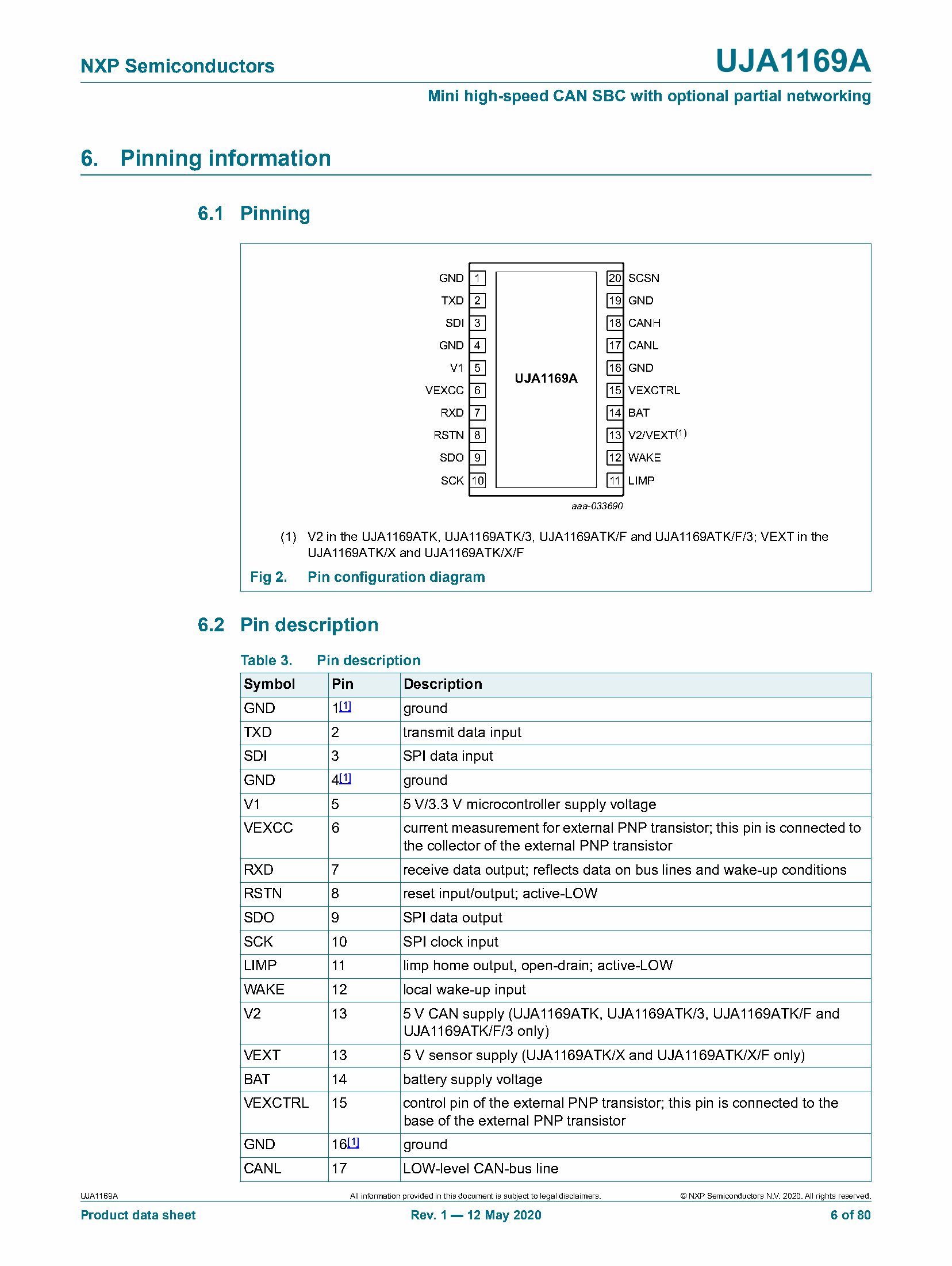
Pinning Information